Update on SVT electronics Giuliana Rizzo INFN and
- Slides: 16

Update on SVT electronics Giuliana Rizzo INFN and University, Pisa on behalf of SLIM 5 -Collaboration & SVT-Super. B group Super. B Workshop - Elba 2008 June 2, 2008 G. Rizzo-Super. B Elba Workshop Electronics Session - June. 2 2008 1

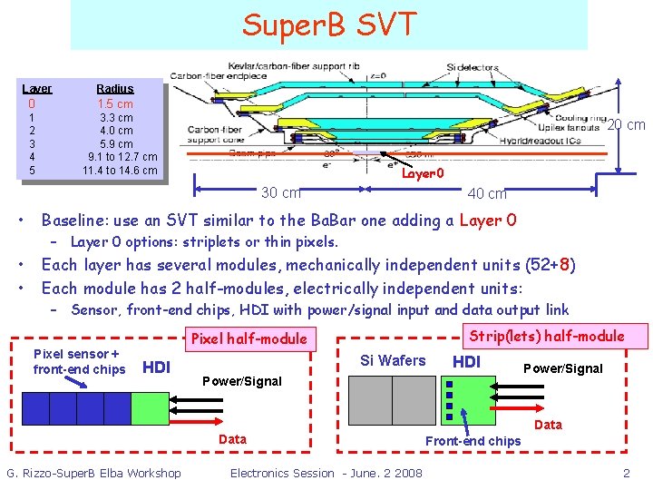
Super. B SVT Layer 0 1 2 3 4 5 Radius 1. 5 cm 3. 3 cm 4. 0 cm 5. 9 cm 9. 1 to 12. 7 cm 11. 4 to 14. 6 cm 20 cm Layer 0 30 cm 40 cm • Baseline: use an SVT similar to the Ba. Bar one adding a Layer 0 • • Each layer has several modules, mechanically independent units (52+8) Each module has 2 half-modules, electrically independent units: – Layer 0 options: striplets or thin pixels. – Sensor, front-end chips, HDI with power/signal input and data output link Pixel sensor + front-end chips Strip(lets) half-module Pixel half-module HDI Si Wafers Power/Signal Data G. Rizzo-Super. B Elba Workshop HDI Electronics Session - June. 2 2008 Power/Signal Data Front-end chips 2

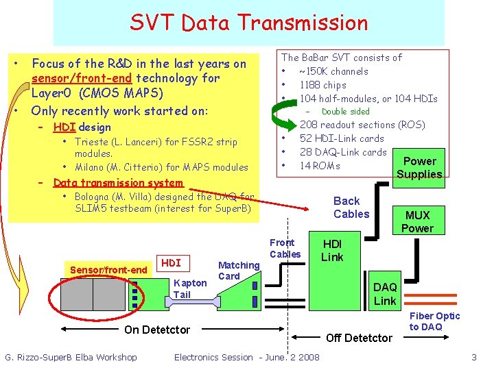
SVT Data Transmission • • Focus of the R&D in the last years on sensor/front-end technology for Layer 0 (CMOS MAPS) Only recently work started on: – HDI design • Trieste (L. Lanceri) for FSSR 2 strip modules. • Milano (M. Citterio) for MAPS modules The Ba. Bar SVT consists of • ~150 K channels • 1188 chips • 104 half-modules, or 104 HDIs – • • Double sided 208 readout sections (ROS) 52 HDI-Link cards 28 DAQ-Link cards Power 14 ROMs Supplies – Data transmission system • Bologna (M. Villa) designed the DAQ for SLIM 5 testbeam (interest for Super. B) Sensor/front-end HDI Kapton Tail Back Cables Front Cables Matching Card On Detetctor G. Rizzo-Super. B Elba Workshop Electronics Session - June. 2 2008 MUX Power HDI Link DAQ Link Off Detetctor Fiber Optic to DAQ 3

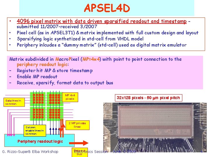
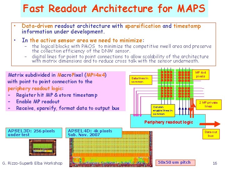
APSEL 4 D • • 4096 pixel matrix with data driven sparsified readout and timestamp - submitted 11/2007 -received 3/2007 Pixel cell (as in APSEL 3 T 1) & matrix implemented with full custom design and layout Sparsifying logic synthetized in std-cell from VHDL model Periphery inlcudes a “dummy matrix” (std-cell) used as digital matrix emulator Matrix subdivided in Macro. Pixel (MP=4 x 4) with point to point connection to the periphery readout logic: – Register hit MP & store timestamp – Enable MP readout – Receive, sparsify, format data to output bus MP 4 x 4 pixels Data lines in common Column enable lines in common 32 x 128 pixels - 50 mm pixel pitch 2 MP private lines Periphery readout logic G. Rizzo-Super. B Elba Workshop Data out Electronics bus Session - June. 2 2008 4

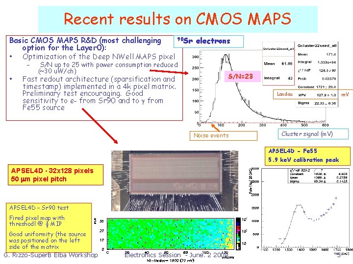
Recent results on CMOS MAPS 90 Sr electrons Basic CMOS MAPS R&D (most challenging option for the Layer 0): • Optimization of the Deep NWell MAPS pixel – • S/N up to 25 with power consumption reduced (~30 u. W/ch) S/N=23 Fast redout architecture (sparsification and timestamp) implemented in a 4 k pixel matrix. Preliminary test encouraging. Good sensitivity to e- from Sr 90 and to g from Fe 55 source Landau Noise events m. V Cluster signal (m. V) APSEL 4 D - Fe 55 5. 9 ke. V calibration peak APSEL 4 D - 32 x 128 pixels 50 mm pixel pitch APSEL 4 D – Sr 90 test Fired pixel map with threshodl @ ½ MIP Good uniformity (the source was positioned on the left side of the matrix G. Rizzo-Super. B Elba Workshop Electronics Session - June. 2 2008 5

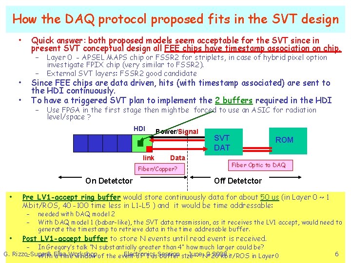
How the DAQ protocol proposed fits in the SVT design • Quick answer: both proposed models seem acceptable for the SVT since in present SVT conceptual design all FEE chips have timestamp association on chip. – – • Layer 0 - APSEL MAPS chip or FSSR 2 for striplets, in case of hybrid pixel option investigate FPIX chip (very similar to FSSR 2). External SVT layers: FSSR 2 good candidate Since FEE chips are data driven, hits (with timestamp associated) are sent to the HDI continuously. To have a triggered SVT plan to implement the 2 buffers required in the HDI • – Use FPGA in the first stage then mightbe forced to use an ASIC for radiation level/space ? HDI link Power/Signal Data Fiber/Copper? On Detetctor • ROM Fiber Optic to DAQ Off Detetctor Pre LV 1 -accept ring buffer would store continuously data for about 50 us (in Layer 0 ~ 1 Mbit/ROS, 40 -100 time less in L 1 -L 5 ) and it would be time addressable: – – • SVT DAT needed with DAQ model 2 With DAQ model 1 (babar-like), the SVT data trasmission, as it receives the LV 1 accept, would need to generate the timestamp to retrieve data in the time addresable buffer. Post LV 1 -accept buffer to store N events until read event is received. – In Gregory’s talk “N substantially greater than 4” how much larger could be? G. Rizzo-Super. B Workshop Electronics - June. 2 2008 – With Elba a time window of the event of 1 us. Session buffer size ~ N*20 kbit/ROS in Layer 0 6

Clocks and readout time window • Time window of the event forced by the shaping time of the front -end. Shaping time 200 ns in MAPS chip as BABAR SVT inner layers • Reasonable time window about 500 ns – 1 us, as in BABAR now. • Readout clock for MAPS chips need to be fast (160 MHz) to cope with the expected background rate (safety included): 160 Mhit/s in each chip and no local buffer. – Could be 80 MHz reducing the chip size by 2 but increasing the module complexity. Need to evaluate this options. • Timestamp counter clock (we call it BC clock) cannot be very fast: in the MAPS architecture pixel are organized in Macro. Pixels (4 x 4) and at each rising edge of the BCO clock the readout freeze all the pixels inside a MP where there was an hit (only 1 timestamp counter/MP available): – The first fired pixel would be the seed of the cluster (more charge) but with a fast BC clock the other pixel in the MP would be immediately freezed and cannot contribute to the cluster. Need to evaluate this effect – BC clock ~ 100 ns is probably OK. G. Rizzo-Super. B Elba Workshop Electronics Session - June. 2 2008 7

Other options • To implement LV 1 trigger with SVT data (Associative Memories): – more intelligence should be added on the Layer 0 hybrid to select and send to AM prompt data but with lower granularity to reduce the link speed needed. • Using the Macro. Pixel granularity (200 x 200 um) the link speed between ROS/DAT should be ~ 1 Gbit/s/ROS. (full granularity means ~ 16 Gbit/s/ROS) – Can use full granularity for external layers • link speed needed is < 1 Gbit/s/ROS • To implement LV 3 trigger track with SVT, triggered events can be send to AM G. Rizzo-Super. B Elba Workshop Electronics Session - June. 2 2008 8

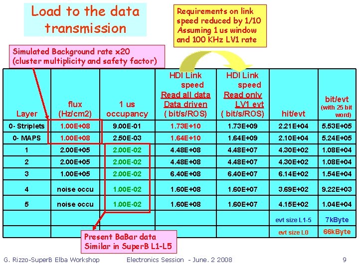
Load to the data transmission Requirements on link speed reduced by 1/10 Assuming 1 us window and 100 KHz LV 1 rate Simulated Background rate x 20 (cluster multiplicity and safety factor) Layer flux (Hz/cm 2) 1 us occupancy HDI Link speed Read all data Data driven ( bit/s/ROS) 0 - Striplets 1. 00 E+08 9. 00 E-01 1. 73 E+10 1. 73 E+09 2. 21 E+04 5. 53 E+05 0 - MAPS 1. 00 E+08 2. 50 E-03 1. 64 E+10 1. 64 E+09 2. 10 E+04 5. 24 E+05 1 2. 00 E+05 2. 00 E-02 4. 48 E+08 4. 48 E+07 4. 30 E+02 1. 08 E+04 2 2. 00 E+05 2. 00 E-02 4. 48 E+08 4. 48 E+07 4. 30 E+02 1. 08 E+04 3 1. 00 E+05 2. 00 E-02 6. 40 E+08 6. 40 E+07 6. 14 E+02 1. 54 E+04 4 noise occu 1. 00 E-02 1. 60 E+08 1. 60 E+07 3. 69 E+02 9. 22 E+03 5 noise occu 1. 00 E-02 1. 60 E+08 1. 60 E+07 4. 15 E+02 1. 04 E+04 evt size L 1 -5 7 k. Byte Present Ba. Bar data Similar in Super. B L 1 -L 5 evt size L 0 66 k. Byte G. Rizzo-Super. B Elba Workshop HDI Link speed Read only LV 1 evt ( bit/s/ROS) hit/evt (with 25 bit word) Electronics Session - June. 2 2008 bit/evt 9

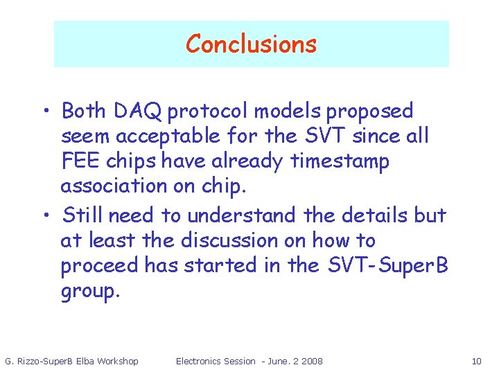
Conclusions • Both DAQ protocol models proposed seem acceptable for the SVT since all FEE chips have already timestamp association on chip. • Still need to understand the details but at least the discussion on how to proceed has started in the SVT-Super. B group. G. Rizzo-Super. B Elba Workshop Electronics Session - June. 2 2008 10

backup G. Rizzo-Super. B Elba Workshop Electronics Session - June. 2 2008 11

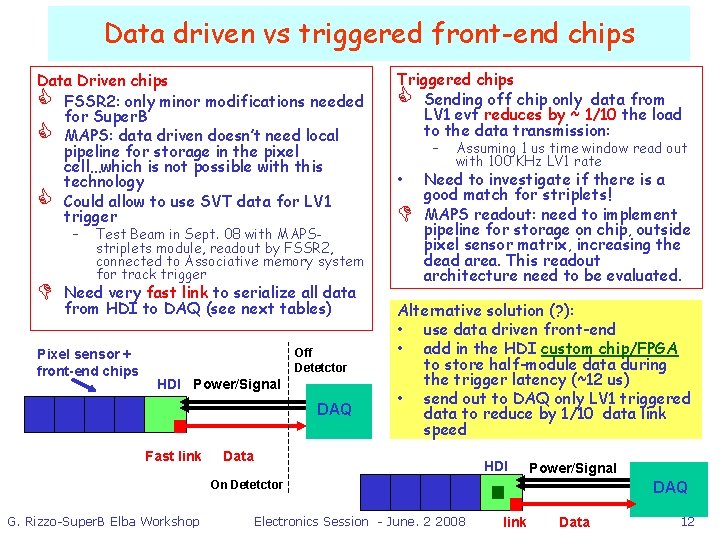
Data driven vs triggered front-end chips Data Driven chips C FSSR 2: only minor modifications needed for Super. B C MAPS: data driven doesn’t need local pipeline for storage in the pixel cell…which is not possible with this technology C Could allow to use SVT data for LV 1 trigger – D Test Beam in Sept. 08 with MAPSstriplets module, readout by FSSR 2, connected to Associative memory system for track trigger Need very fast link to serialize all data from HDI to DAQ (see next tables) Pixel sensor + front-end chips Off Detetctor HDI Power/Signal DAQ Fast link Triggered chips C Sending off chip only data from LV 1 evt reduces by ~ 1/10 the load to the data transmission: – • D Assuming 1 us time window read out with 100 KHz LV 1 rate Need to investigate if there is a good match for striplets! MAPS readout: need to implement pipeline for storage on chip, outside pixel sensor matrix, increasing the dead area. This readout architecture need to be evaluated. Alternative solution (? ): • use data driven front-end • add in the HDI custom chip/FPGA to store half-module data during the trigger latency (~12 us) • send out to DAQ only LV 1 triggered data to reduce by 1/10 data link speed Data HDI Power/Signal On Detetctor G. Rizzo-Super. B Elba Workshop Electronics Session - June. 2 2008 DAQ link Data 12

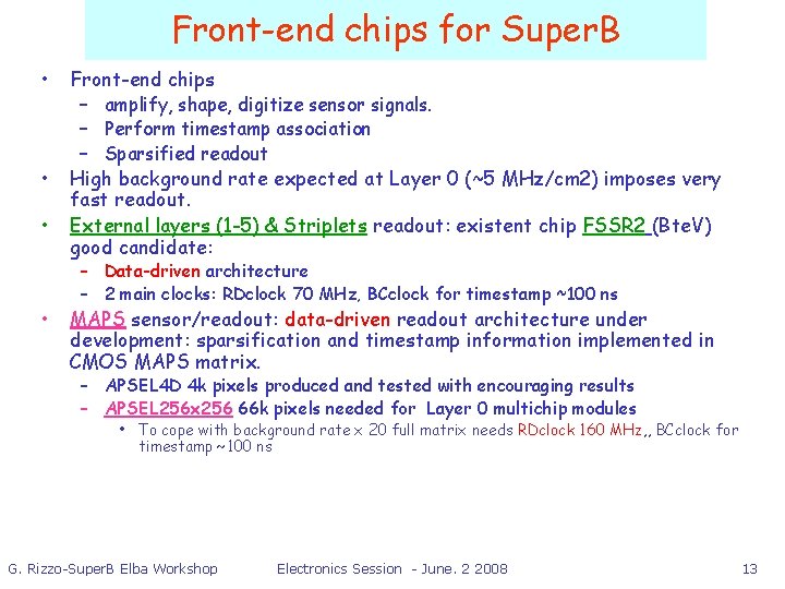
Front-end chips for Super. B • • Front-end chips – amplify, shape, digitize sensor signals. – Perform timestamp association – Sparsified readout High background rate expected at Layer 0 (~5 MHz/cm 2) imposes very fast readout. External layers (1 -5) & Striplets readout: existent chip FSSR 2 (Bte. V) good candidate: – Data-driven architecture – 2 main clocks: RDclock 70 MHz, BCclock for timestamp ~100 ns MAPS sensor/readout: data-driven readout architecture under development: sparsification and timestamp information implemented in CMOS MAPS matrix. – APSEL 4 D 4 k pixels produced and tested with encouraging results – APSEL 256 x 256 66 k pixels needed for Layer 0 multichip modules • To cope with background rate x 20 full matrix needs RDclock 160 MHz, , BCclock for timestamp ~100 ns G. Rizzo-Super. B Elba Workshop Electronics Session - June. 2 2008 13

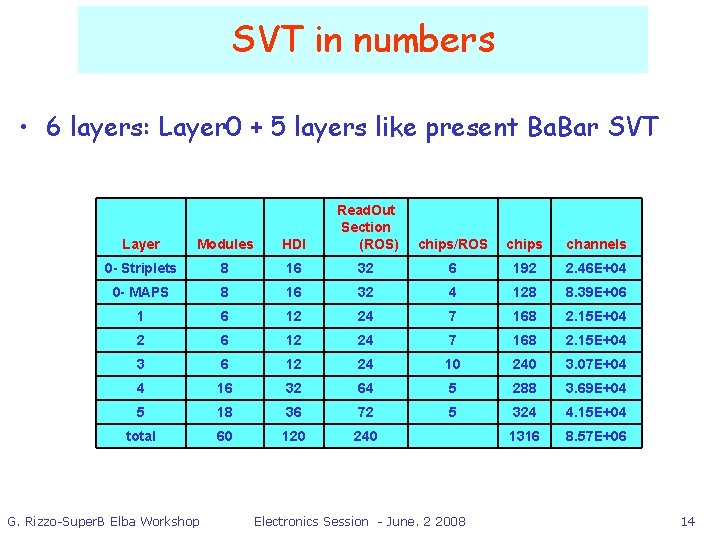
SVT in numbers • 6 layers: Layer 0 + 5 layers like present Ba. Bar SVT Layer Modules HDI Read. Out Section (ROS) 0 - Striplets 8 16 32 6 192 2. 46 E+04 0 - MAPS 8 16 32 4 128 8. 39 E+06 1 6 12 24 7 168 2. 15 E+04 2 6 12 24 7 168 2. 15 E+04 3 6 12 24 10 240 3. 07 E+04 4 16 32 64 5 288 3. 69 E+04 5 18 36 72 5 324 4. 15 E+04 total 60 120 240 1316 8. 57 E+06 G. Rizzo-Super. B Elba Workshop chips/ROS chips channels Electronics Session - June. 2 2008 14

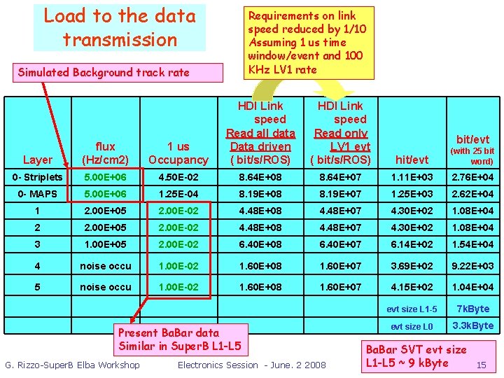
Load to the data transmission Requirements on link speed reduced by 1/10 Assuming 1 us time window/event and 100 KHz LV 1 rate Simulated Background track rate Layer flux (Hz/cm 2) 1 us Occupancy HDI Link speed Read all data Data driven ( bit/s/ROS) 0 - Striplets 5. 00 E+06 4. 50 E-02 8. 64 E+08 8. 64 E+07 1. 11 E+03 2. 76 E+04 0 - MAPS 5. 00 E+06 1. 25 E-04 8. 19 E+08 8. 19 E+07 1. 25 E+03 2. 62 E+04 1 2. 00 E+05 2. 00 E-02 4. 48 E+08 4. 48 E+07 4. 30 E+02 1. 08 E+04 2 2. 00 E+05 2. 00 E-02 4. 48 E+08 4. 48 E+07 4. 30 E+02 1. 08 E+04 3 1. 00 E+05 2. 00 E-02 6. 40 E+08 6. 40 E+07 6. 14 E+02 1. 54 E+04 4 noise occu 1. 00 E-02 1. 60 E+08 1. 60 E+07 3. 69 E+02 9. 22 E+03 5 noise occu 1. 00 E-02 1. 60 E+08 1. 60 E+07 4. 15 E+02 1. 04 E+04 evt size L 1 -5 7 k. Byte Present Ba. Bar data Similar in Super. B L 1 -L 5 evt size L 0 3. 3 k. Byte G. Rizzo-Super. B Elba Workshop HDI Link speed Read only LV 1 evt ( bit/s/ROS) hit/evt (with 25 bit word) Electronics Session - June. 2 2008 bit/evt Ba. Bar SVT evt size L 1 -L 5 ~ 9 k. Byte 15

Fast Readout Architecture for MAPS • Data-driven readout architecture with sparsification and timestamp information under development. • In the active sensor area we need to minimize: – – the logical blocks with PMOS to minimize the competitive nwell area and preserve the collection efficiency of the DNW sensor. digital lines for point to point connections to allow scalability of the architecture with matrix dimensions and to reduce cross talk with the sensor underneath. Matrix subdivided in Macro. Pixel (MP=4 x 4) with point to point connection to the periphery readout logic: – Register hit MP & store timestamp – Enable MP readout – Receive, sparsify, format data to output bus MP 4 x 4 pixels Data lines in common Column enable lines in common 2 MP private lines Periphery readout logic APSEL 3 D: 256 pixels under test G. Rizzo-Super. B Elba Workshop APSEL 4 D: 4 k pixels Data out bus Sub. Nov. 2007 Electronics Session - June. 2 2008 50 x 50 um pitch 16