SVT detector electronics Filippo Giorgi INFN Universit di
- Slides: 12

SVT detector electronics Filippo Giorgi INFN & Università di Bologna Overview: - Super. B SVT - Layer 0 peculiarities - SVT channels and reading chains - Rate, links and event size

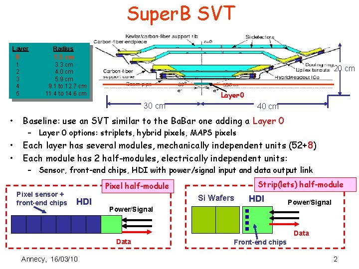
Super. B SVT Layer Radius 0 1. 5 cm 1 2 3 4 5 3. 3 cm 4. 0 cm 5. 9 cm 9. 1 to 12. 7 cm 11. 4 to 14. 6 cm 20 cm Layer 0 30 cm 40 cm • Baseline: use an SVT similar to the Ba. Bar one adding a Layer 0 • • Each layer has several modules, mechanically independent units (52+8) Each module has 2 half-modules, electrically independent units: – Layer 0 options: striplets, hybrid pixels, MAPS pixels – Sensor, front-end chips, HDI with power/signal input and data output link Pixel sensor + front-end chips Strip(lets) half-module Pixel half-module HDI Si Wafers HDI Power/Signal Data Annecy, 16/03/10 Front-end chips 2

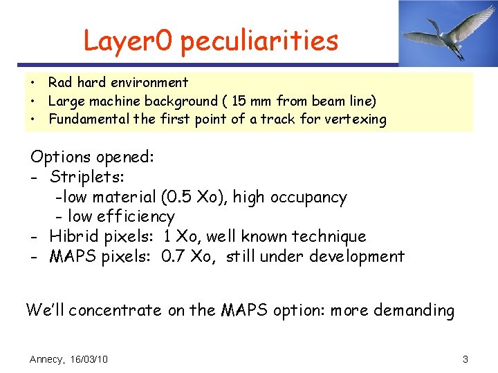
Layer 0 peculiarities • Rad hard environment • Large machine background ( 15 mm from beam line) • Fundamental the first point of a track for vertexing Options opened: - Striplets: -low material (0. 5 Xo), high occupancy - low efficiency - Hibrid pixels: 1 Xo, well known technique - MAPS pixels: 0. 7 Xo, still under development We’ll concentrate on the MAPS option: more demanding Annecy, 16/03/10 3

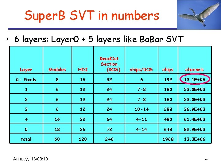
Super. B SVT in numbers • 6 layers: Layer 0 + 5 layers like Ba. Bar SVT Layer Modules HDI Read. Out Section (ROS) 0 - Pixels 8 16 32 6 192 13. 1 E+06 1 6 12 24 7 -8 180 23. 0 E+03 2 6 12 24 7 -8 180 23. 0 E+03 3 6 12 24 10 -14 288 36. 9 E+03 4 16 32 64 4 -11 480 61. 4 E+03 5 18 36 72 4 -14 648 82. 9 E+03 total 60 120 240 1968 13. 3 E+06 Annecy, 16/03/10 chips/ROS chips channels 4

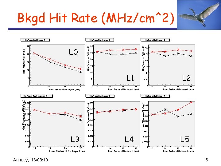
Bkgd Hit Rate (MHz/cm^2) L 0 L 3 Annecy, 16/03/10 L 1 L 2 L 4 L 5 5

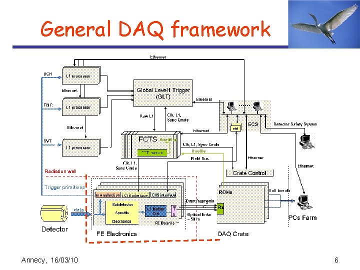
General DAQ framework Annecy, 16/03/10 6

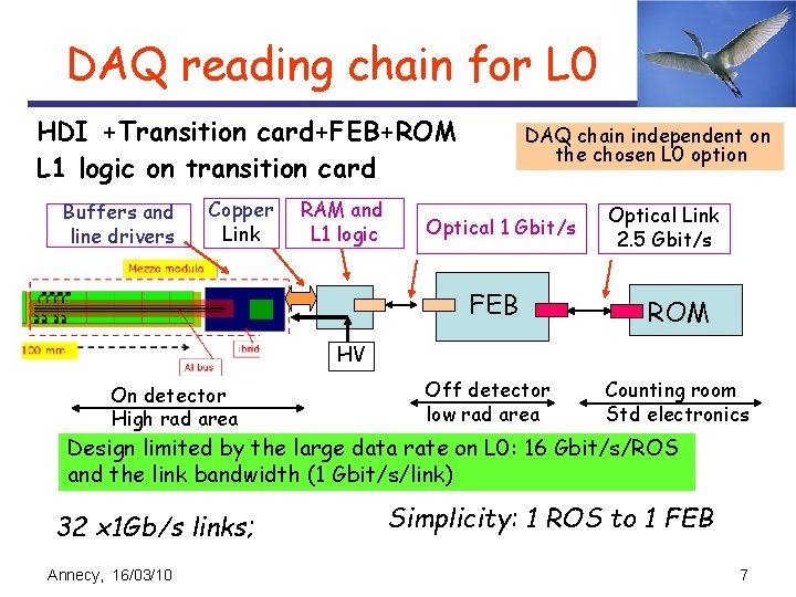
DAQ reading chain for L 0 HDI +Transition card+FEB+ROM L 1 logic on transition card Buffers and line drivers Copper Link RAM and L 1 logic DAQ chain independent on the chosen L 0 option Optical 1 Gbit/s Optical Link 2. 5 Gbit/s FEB ROM Off detector low rad area Counting room Std electronics HV On detector High rad area Design limited by the large data rate on L 0: 16 Gbit/s/ROS and the link bandwidth (1 Gbit/s/link) 32 x 1 Gb/s links; Annecy, 16/03/10 Simplicity: 1 ROS to 1 FEB 7

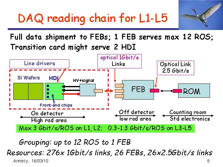
DAQ reading chain for L 1 -L 5 Full data shipment to FEBs; 1 FEB serves max 12 ROS; Transition card might serve 2 HDI optical 1 Gbit/s Links Line drivers Si Wafers HDI Optical Link 2. 5 Gbit/s HV+signal FEB ROM Front-end chips On detector High rad area Off detector low rad area Counting room Std electronics Max 3 Gbit/s/ROS on L 1, L 2; 0. 3 -1. 3 Gbit/s/ROS on L 3 -L 5 Grouping: up to 12 ROS to 1 FEB Resources: 276 x 1 Gbit/s links, 26 FEBs, 26 x 2. 5 Gbit/s links Annecy, 16/03/10 8

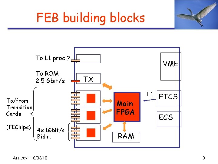
FEB building blocks To L 1 proc ? To ROM 2. 5 Gbit/s To/from Transition Cards (FEChips) VME TX Main FPGA 4 x 1 Gbit/s Bidir. Annecy, 16/03/10 L 1 FTCS ECS RAM 9

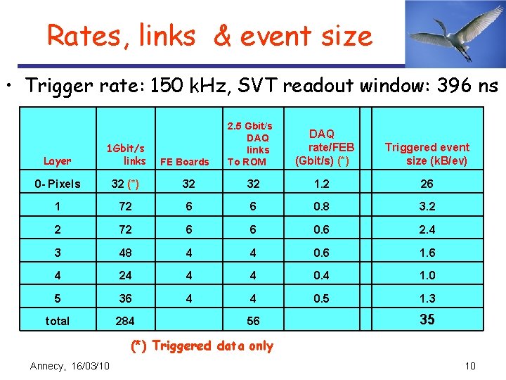
Rates, links & event size • Trigger rate: 150 k. Hz, SVT readout window: 396 ns 2. 5 Gbit/s DAQ links To ROM DAQ rate/FEB (Gbit/s) (*) Triggered event size (k. B/ev) Layer 1 Gbit/s links 0 - Pixels 32 (*) 32 32 1. 2 26 1 72 6 6 0. 8 3. 2 2 72 6 6 0. 6 2. 4 3 48 4 4 0. 6 1. 6 4 24 4 4 0. 4 1. 0 5 36 4 4 0. 5 1. 3 total 284 FE Boards 56 35 (*) Triggered data only Annecy, 16/03/10 10

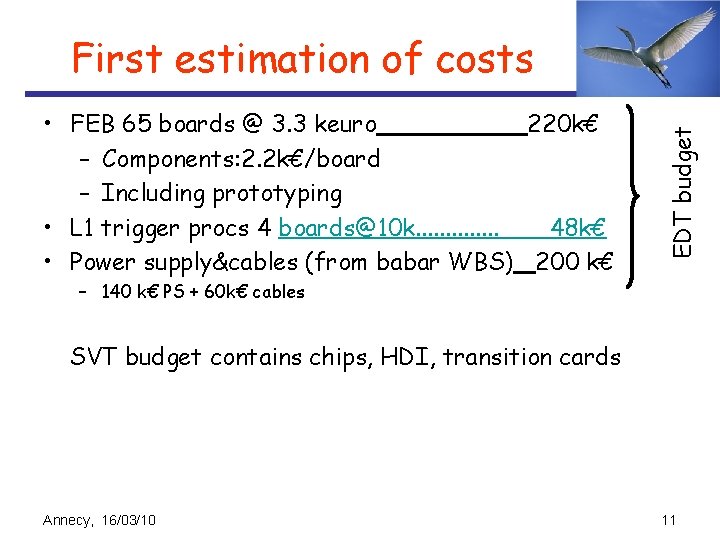
• FEB 65 boards @ 3. 3 keuro 220 k€ – Components: 2. 2 k€/board – Including prototyping • L 1 trigger procs 4 boards@10 k. . . 48 k€ • Power supply&cables (from babar WBS) 200 k€ EDT budget First estimation of costs – 140 k€ PS + 60 k€ cables SVT budget contains chips, HDI, transition cards Annecy, 16/03/10 11

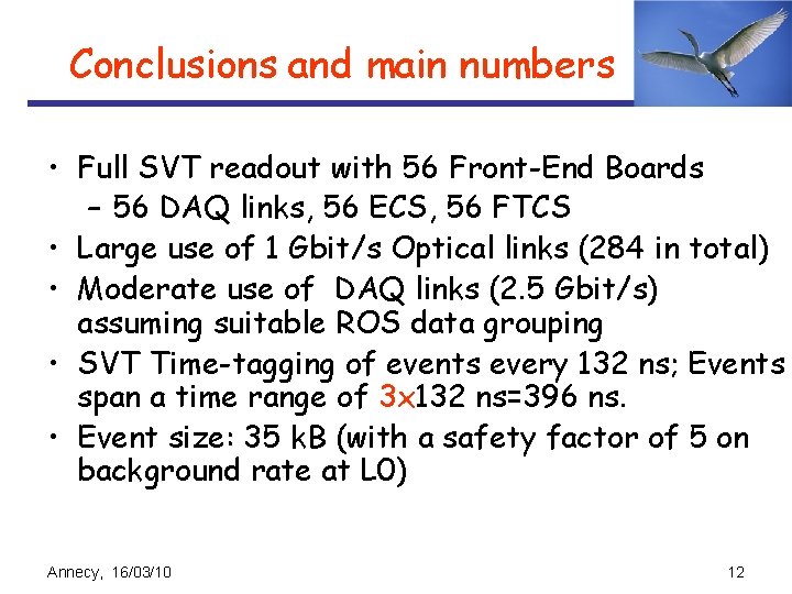
Conclusions and main numbers • Full SVT readout with 56 Front-End Boards – 56 DAQ links, 56 ECS, 56 FTCS • Large use of 1 Gbit/s Optical links (284 in total) • Moderate use of DAQ links (2. 5 Gbit/s) assuming suitable ROS data grouping • SVT Time-tagging of events every 132 ns; Events span a time range of 3 x 132 ns=396 ns. • Event size: 35 k. B (with a safety factor of 5 on background rate at L 0) Annecy, 16/03/10 12