SVT frontend electronics Mauro Citterio INFN Milano On
- Slides: 13

SVT front-end electronics Mauro Citterio INFN Milano On behalf of SVT group Mauro Citterio - EDT Parallel meeting – Super. B Workshop, Perugia - June 18, 2009 1

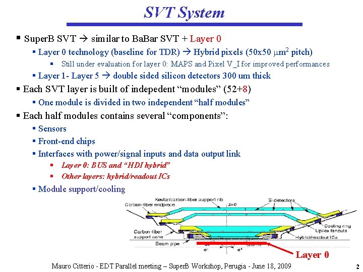
SVT System § Super. B SVT similar to Ba. Bar SVT + Layer 0 § Layer 0 technology (baseline for TDR) Hybrid pixels (50 x 50 mm 2 pitch) § Still under evaluation for layer 0: MAPS and Pixel V_I for improved performances § Layer 1 - Layer 5 double sided silicon detectors 300 um thick § Each SVT layer is built of indepedent “modules” (52+8) § One module is divided in two independent “half modules” § Each half modules contains several “components”: § Sensors § Front-end chips § Interfaces with power/signal inputs and data output link § Layer 0: BUS and “HDI hybrid” § Other layers: hybrid/readout ICs § Module support/cooling Layer 0 Mauro Citterio - EDT Parallel meeting – Super. B Workshop, Perugia - June 18, 2009 2

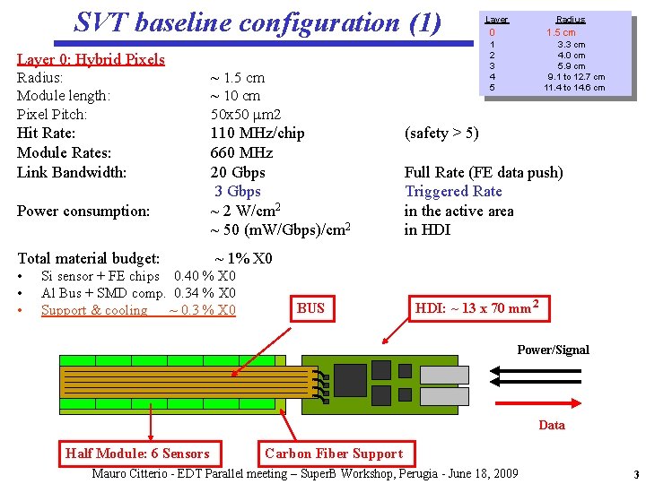
SVT baseline configuration (1) Radius: Module length: Pixel Pitch: ~ 1. 5 cm ~ 10 cm 50 x 50 mm 2 Hit Rate: Module Rates: Link Bandwidth: 110 MHz/chip 660 MHz 20 Gbps 3 Gbps ~ 2 W/cm 2 ~ 50 (m. W/Gbps)/cm 2 Total material budget: • • • Radius 0 1. 5 cm 1 2 3 4 5 Layer 0: Hybrid Pixels Power consumption: Layer 3. 3 cm 4. 0 cm 5. 9 cm 9. 1 to 12. 7 cm 11. 4 to 14. 6 cm (safety > 5) Full Rate (FE data push) Triggered Rate in the active area in HDI ~ 1% X 0 Si sensor + FE chips 0. 40 % X 0 Al Bus + SMD comp. 0. 34 % X 0 Support & cooling ~ 0. 3 % X 0 BUS HDI: ~ 13 x 70 mm 2 Power/Signal Data Half Module: 6 Sensors Carbon Fiber Support Mauro Citterio - EDT Parallel meeting – Super. B Workshop, Perugia - June 18, 2009 3

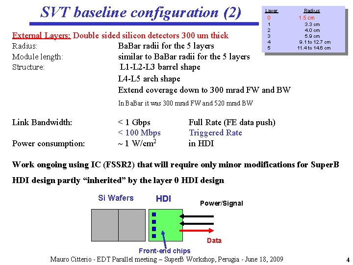
SVT baseline configuration (2) Layer 0 1 2 3 4 5 External Layers: Double sided silicon detectors 300 um thick Radius: Ba. Bar radii for the 5 layers Module length: similar to Ba. Bar radii for the 5 layers Structure: L 1 -L 2 -L 3 barrel shape L 4 -L 5 arch shape Extend coverage down to 300 mrad FW and BW Radius 1. 5 cm 3. 3 cm 4. 0 cm 5. 9 cm 9. 1 to 12. 7 cm 11. 4 to 14. 6 cm In Ba. Bar it was 300 mrad FW and 520 mrad BW Link Bandwidth: Power consumption: < 1 Gbps < 100 Mbps ~ 1 W/cm 2 Full Rate (FE data push) Triggered Rate in HDI Work ongoing using IC (FSSR 2) that will require only minor modifications for Super. B HDI design partly “inherited” by the layer 0 HDI design Si Wafers HDI Power/Signal Data Front-end chips Mauro Citterio - EDT Parallel meeting – Super. B Workshop, Perugia - June 18, 2009 4

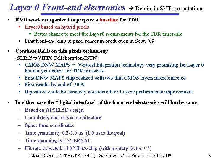
Layer 0 Front-end electronics Details in SVT presentations § R&D work reorganized to prepare a baseline for TDR § Layer 0 based on hybrid pixels § Better chance to meet the Layer 0 requirements for the TDR timescale § First front-end chip & pixel sensor in production in Sept. ’ 09 § Continue R&D on thin pixels technology (SLIM 5 VIPIX Collaboration-INFN) § CMOS DNW MAPS + Vertical Integration technology very promising for Layer 0 but not yet mature for TDR timescale. § First DNW MAPS chip realized with two thin CMOS layers interconnected § First results by end of 2009 § If positive could be seriously considered for Layer 0 performance improvement • In either case the “digital interface” of the front-end electronics will be the same – Based on APSEL 5 D design – Completely data driven architecture – Space time coordinates – Time granularity 0. 2 -5. 0 us (1. 0 us is the goal) – Time stamping is EXTERNAL. – Hit rate expected: 110 Mhit/s/chip (with a safety factor > 5) Mauro Citterio - EDT Parallel meeting – Super. B Workshop, Perugia - June 18, 2009 5

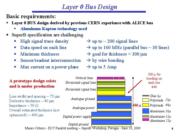
Layer 0 Bus Design Basic requirements: § Layer 0 BUS design derived by previous CERN experience with ALICE bus § Aluminum-Kapton technology used § Super. B specification are challenging § High signal trace density § Data speed on each line § Minimum thickness § Sensor/readout interconnection § Max current on a power plane A prototype design exists and is under production up to ~ 200 signal lines up to 160 MHz (parallel bus ~ 30 lines) goal for thickness < 300 mm by wire bonding up to 5 Amp 300 m for bonding on each bus side Vertical lines Horizontal signal lines Line widht and spacing ~ 75 mm Analogue ground Dielectric thickness ~ 40 mm Impedance ~ 50 W Analogue power Overall estimated thickness (not optimized!) ~ 400 mm Digital power supply 400 µ Digital ground Mauro Citterio - EDT Parallel meeting – Super. B Workshop, Perugia - June 18, 2009 Glue 5µ Polyimide 15µ Polyimide 40µ Aluminium 50µ Aluminium 13µ 6

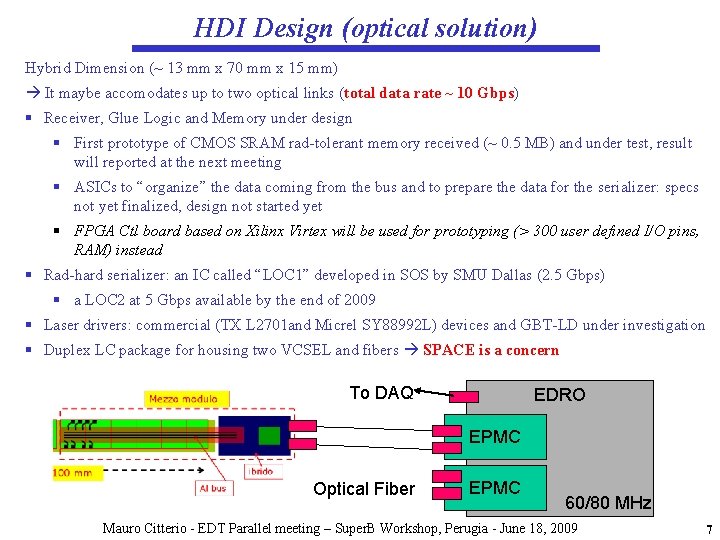
HDI Design (optical solution) Hybrid Dimension (~ 13 mm x 70 mm x 15 mm) It maybe accomodates up to two optical links (total data rate ~ 10 Gbps) § Receiver, Glue Logic and Memory under design § First prototype of CMOS SRAM rad-tolerant memory received (~ 0. 5 MB) and under test, result will reported at the next meeting § ASICs to “organize” the data coming from the bus and to prepare the data for the serializer: specs not yet finalized, design not started yet § FPGA Ctl board based on Xilinx Virtex will be used for prototyping (> 300 user defined I/O pins, RAM) instead § Rad-hard serializer: an IC called “LOC 1” developed in SOS by SMU Dallas (2. 5 Gbps) § a LOC 2 at 5 Gbps available by the end of 2009 § Laser drivers: commercial (TX L 2701 and Micrel SY 88992 L) devices and GBT-LD under investigation § Duplex LC package for housing two VCSEL and fibers SPACE is a concern To DAQ EDRO EPMC Optical Fiber EPMC 60/80 MHz Mauro Citterio - EDT Parallel meeting – Super. B Workshop, Perugia - June 18, 2009 7

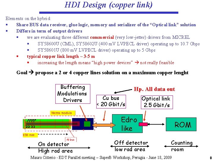
HDI Design (copper link) Elements on the hybrid: § Share BUS data receiver, glue logic, memory and serializer of the “Optical link” solution § Differs in term of output drivers § we are evaluating three different commercial (very low-jetter) drivers from MICREL § SY 58600 U (CML), SY 58602 U (400 m. V LVPECL driver) operating up to 10. 7 Gbps § SY 58601 U (800 m. V LVPECL driver) operating up to 5 Gbps § typical copper link length ~ 3 -5 m § increasing the length means “high power devices” not really feasible Goal propose a 2 or 4 copper lines solution on a maximum copper lenght Buffering Modulations Drivers Hp. All data out Cu bus < 20 Gbit/s Optical link 2. 5 Gbit/s Edro like On detector High rad area Off detector low rad area ROM Counting room Mauro Citterio - EDT Parallel meeting – Super. B Workshop, Perugia - June 18, 2009 8

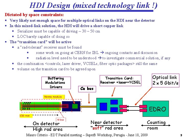
HDI Design (mixed technology link !) Dictated by space constraints: § Very likely not enough space for multiple optical links on the HDI near the detector § In this mixed-link solution, the HDI will drive a short copper link § Serializer must be capable of driving ~ 30 – 50 cm § LOC barely capable of doing so § The “transition card” will be active § a “rad-tolerant” receiver must be found § some work on going at CERN for IBL ongoing contacts and discussion § radiation level need to be understood to investigate commercial solution, if any § the combination <controls, laser driver, VCSELs, fiber optic packages> still the same § volume on the transition card to be agreed upon Buffering Modulations Drivers Optical link 2 x 5 Gbit/s Transition Card: Receiver +laser+VCSEL Cu bus EDRO On detector High rad area Near detector “soft” rad area Counting room Mauro Citterio - EDT Parallel meeting – Super. B Workshop, Perugia - June 18, 2009 9

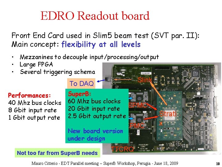
EDRO Readout board Front End Card used in Slim 5 beam test (SVT par. II): Main concept: flexibility at all levels • Mezzanines to decouple input/processing/output • Large FPGA • Several triggering schema Slink To DAQ Performances: 40 Mhz bus clocks 8 Gbit input rate 1 Gbit output rate Super. B: 60 Data Mhzfrom bus clocks chips 20 FE Gbit input rate EPMC Gbit/soutput rate 2. 54 Gbit New board version 2. 5 ME/s evaluated @L 1 under design 40 k. Hz DAQ rate @slim 5 Not too far from Super. B needs EPMC Strati x TTCRQ Mauro Citterio - EDT Parallel meeting – Super. B Workshop, Perugia - June 18, 2009 10

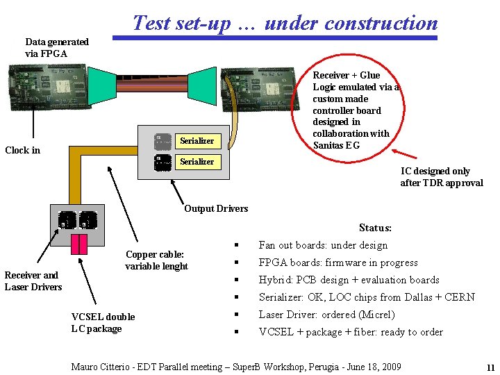
Test set-up … under construction Data generated via FPGA Receiver + Glue Logic emulated via a custom made controller board designed in collaboration with Sanitas EG Serializer Clock in Serializer IC designed only after TDR approval Output Drivers Status: Receiver and Laser Drivers Copper cable: variable lenght VCSEL double LC package § Fan out boards: under design § FPGA boards: firmware in progress § Hybrid: PCB design + evaluation boards § Serializer: OK, LOC chips from Dallas + CERN § Laser Driver: ordered (Micrel) § VCSEL + package + fiber: ready to order Mauro Citterio - EDT Parallel meeting – Super. B Workshop, Perugia - June 18, 2009 11

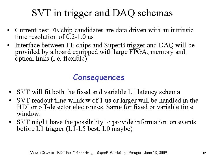
SVT in trigger and DAQ schemas • Current best FE chip candidates are data driven with an intrinsic time resolution of 0. 2 -1. 0 us • Interface between FE chips and Super. B trigger and DAQ will be provided by a board equipped with large FPGA, memory and optical links (i. e. flexible) Consequences • SVT will fit both the fixed and variable L 1 latency schema • SVT readout time window of 1 us or larger will be handled in the HDI or off-detector electronics. Same for fixed or variable time window. • SVT might have the possibility to provide information on events before L 1 trigger (L 1 -L 5 best, L 0 maybe) Mauro Citterio - EDT Parallel meeting – Super. B Workshop, Perugia - June 18, 2009 12

Conclusions • Main SVT challenge: layer 0 – rates, chips, data bus and data transmission • Current best FE chip candidates are data driven • Front End Card and/or HDIs with enough logic to fit different DAQ and L 1 schemas • Trigger rate >150 k. Hz, time window >=1 us • Data volume: – L 1 -L 5: 6 k. B with 1 us time window – L 0: 66 k. Bytes with 1 us time window and >5 safety factor • SVT in trigger still conceivable, but extremely difficult Mauro Citterio - EDT Parallel meeting – Super. B Workshop, Perugia - June 18, 2009 13