Startup VDD M 3 VDD M 1 When

 and a positively")


k. T/q VDD VDD 1: 1 Dvbe/R - + Vbe 1 R")


- Slides: 19
Start-up VDD M 3 VDD M 1 When Vd 4=Vg 4 < Vdd-|Vtp|, want Ms off M 4 Ms When Vd 4=Vg 4 > Vdd-|Vtp|, want Ms on VB make VB ~ Vdd 2|Vtp| to Vdd-2|Vtp|-Veff M 2 Also make IQ in right branch to be very small.
Temperature independent reference Generate a negatively PTAT (Proportional To Absolute Temperature) and a positively PTAT quantities and sum them appropriately. X can be voltage or current
Bandgap voltage reference Works in bipolar or Bi. CMOS Chapter 7 Figure 09
A Common way of bandgap reference This is easily available in digital CMOS DVBE k. T/q
VBE has negative temp coeff at roughly -2. 2 m. V/°C at room temperature, called CTAT or NTAT Vt = k. T/q is PTAT that has a temperature coefficient of +0. 085 m. V/°C at room temperature. Multiply Vt by a constant K and sum it with the VBE to get VREF = VBE + KVt If K is right (2. 2/0. 085 26), temperature coefficient can be zero.
In general, use VBE + VPTAT
Bandgap reference still varies a little with temp
How to get Bipolar in CMOS?
Layout P-active is E N-well is B P-substrate is C Tie both n-well and p-substrate to Vss Issues: this will not pass LVS Cadence does not know how to simulate
DVbe = ln(n)k. T/q VDD VDD 1: 1 Dvbe/R - + Vbe 1 R Vbe 2 Q + DVbe n. Q Ise. Vbe 1/vth = n. Ise. Vbe 2/vth + x. R x. DVbe n. Q Vref = x. DVbe + Vbe = xln(n)k. T/q + Vbe = xln(n)0. 026 + 0. 6
VDD VDD 1: 1 Vref - + R Q x. R 8 Q 8 Q
Design Steps • Convenient ratio: n=8 • Select desired current I (e. g. 10 u. A) • Select R by making I = ln(n)k. T/q/R R = ln(8)*26 m. V/10 u. A • Select x. R to make Vref = 1. 26 V x = 0. 65 V/26 m. V/ln(8) • Trim x. R to make Vref correct
Adding more degrees of freedom VDD VDD m: 1 1: r Vref - + R Q n. Q x. R n. Q
R 1 and R 3 equal and equal to x. R 2 Q 2 = n. Q 1 Design steps are identical to before. Chapter 7 Figure 13
These are popular structures, but not doable in CMOS Chapter 7 Figure 11 Chapter 7 Figure 10
Cascoded CM Cascoded CG amplifier
Chapter 7 Figure 15
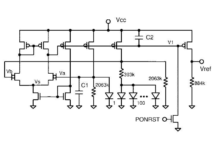
Banba, Hironori, Hitoshi Shiga, Akira Umezawa, Takeshi Miyaba, Toru Tanzawa, Shigeru Atsumi, and Koji Sakui. "A CMOS bandgap reference circuit with sub-1 -V operation. " Solid-State Circuits, IEEE Journal of 34, no. 5 (1999): 670 -674.