Research and Development on High Purity Materials Challenges


 Percent Major (%) Percent Impurity Parts per million (ppm)")


 300 mm single crystal Bonn Germany (July 2002) Year Diameter in")
 (Polish scientist) William Gardner Pfann (27")


 Insoluble inert anode (usually made of a noble or passivated")
 Vacuum Fusion at 800ºC Impurities Gallium")


 unit induction heating equipment High purity quartz tube with glassy carbon")
 Organometallic Precursors (e. g.")


![[In{Se. C 5 H 3(3 -Me)N}3] [Cu{Se. C 5 H 3(Me-3)N}]4 Cu. In. Se](https://slidetodoc.com/presentation_image/4e797b1e9fa5195554cba37674d9a242/image-27.jpg "[In{Se. C 5 H 3(3 -Me)N}3] [Cu{Se. C 5 H 3(Me-3)N}]4 Cu. In. Se")
![[Me 2 Sn(2 -Se. C 5 H 4 N)2] [t. Bu 2 Sn(2 -Se.](https://slidetodoc.com/presentation_image/4e797b1e9fa5195554cba37674d9a242/image-28.jpg "[Me 2 Sn(2 -Se. C 5 H 4 N)2] [t. Bu 2 Sn(2 -Se.")

![[Sb{Se-C 5 H 3(Me-3)N}3]. 2 H 2 O SEM image of uniformly coated antimony](https://slidetodoc.com/presentation_image/4e797b1e9fa5195554cba37674d9a242/image-30.jpg "[Sb{Se-C 5 H 3(Me-3)N}3]. 2 H 2 O SEM image of uniformly coated antimony")


 Technology What next? molecules materials machines")

- Slides: 34
Research and Development on High Purity Materials: Challenges and Opportunities Vimal K. Jain Chemistry Division Bhabha Atomic Research Centre Mumbai (India) email : jainvk@barc. gov. in
TIFR-ASET website This famous 4 th century iron pillar stands in the courtyard of the Quwwatu'l-Islam mosque located in the Qutb Minar complex, Delhi. It was supposedly set up as a standard or dhvaja of god Vishnu on the hill known as Vishnupada, in memory of the mighty king, Chandragupta II (375 -413 AD) of the imperial Gupta dynasty. The total length of this pillar is 7. 2 m, of which 93 cm is buried below the The metal of the pillar has been found to be almost pure malleable iron. The manufacture of such a massive iron pillar, which has not ground. deteriorated much during sixteen hundred years of its existence, is a standing testimony to the Advances in Science, Engineering and Technology (ASET) of ancient India.
Ideally, a high purity material is comprised of atoms of the basic substance, which are arranged in a perfect, periodically repeated structure without any disturbances. Such a perfect crystal is free from extrinsic and intrinsic defects, vacancies, stacking faults, dislocations, interstitial atoms, etc. In contrast, a real crystal is referred to a highly pure substance if there is no difference between its properties and those of the ideal crystal. Thus in practice the definition of ‘high purity’ depends on the sensitivity and the limit of detection of tests and analytical methods. Compositional characterization of matrix is often referred to purity levels. However, materials can also be evaluated with respect to the property of interest
Optical e. g. , Luminescence in phophors Semiconductor Grade Purity Mechanical e. g. , Si, Ge, Ga, As, etc. e. g. , Shape memory alloys Electrical e. g. , Resistivity, electron mobility Magnetic e. g. , Magneto-resistivity in superconducting materials Purpose Oriented Purity Property oriented purity Nuclear Grade Purity e. g. , Zr with extremely low Hf contents Compositional purity Phase purity Purity Si. O 2 : quartz; amorphous; silica gel; insulator layers Carbon : diamond; graphite; fullerene Isotopic purity e. g. , D 2 O, 235 U, etc.
Trace Impurities - Definition (%) Percent Major (%) Percent Impurity Parts per million (ppm) Parts per billion (ppb) 99. 9 (3 N) 0. 1 1000 99. 99 (4 N) 0. 01 100 99. 999 (5 N) 0. 001 10 99. 9999 (6 N) 0. 0001 1 1000 99. 99999 (7 N) 0. 00001 0. 1 100 99. 999999 (8 N) 0. 000001 0. 01 10 99. 9999999 (9 N) 0. 0000001 0. 001 1 (1 mg impurity in 1 Kg) (1 mg impurity in 1 tone)
Prof. J. Bardeen 1 st Generation: Valves 3 rd Generation Small Scale Integrated Circuits (SSI): Less than 100 Transistors per Integrated Circuit or chip Medium Scale Integrated Circuits (MSI): 100 to 1000 Transistors per Integrated Circuit or chip Prof. W. H. Brattain Prof. W. Shockley Bell Labs, USA Nobel Prize in Physics -1956 4 th Generation Large Scale Integrated Circuits (LSI): 1000 to 10000 Transistors per Integrated Circuit or chip Very Large Scale Integrated Circuits (VLSI): 10000 to 1 million Transistors per Integrated Circuit or chip 2 nd Generation: Semiconductor Devices, Diode and single Transistor 5 th Generation Ultra Large Scale Integrated Circuits (ULSI): over 1 million Transistors per Integrated Circuit or Chip 6 th Generation Name of this technology yet to be determined: Over one billion transistors per Integrated Circuit or Chip
Significance of purity Prof. Jack Kilby Texas Instruments Prof. Robert Noyce Fairchild Semiconductor Corp. Noble Prize in Physics - 2000 Effect of heavy metal impurity on large scale integration (LSI) for silicon based devices Dimp (cm-3) deep level Discrete device yield Large Scale Integration Yield 102 104 106 # 1015 (7 N) 0 0 1013 (9 N) 0. 99 0. 37 0 0 1012 (10 N) 0. 999 0. 37 0 1011 (11 N) 0. 999999 0. 37 Dimp - density of heavy metal impurity # Integration level for silicon
Silicon (9 N) 300 mm single crystal Bonn Germany (July 2002) Year Diameter in mm Weight in kg 1950 12 (½”) 0. 05 1956 25 (1”) 0. 4 1962 36 (1. 5” 1. 2 1967 50 (2”) 2. 5 1972 62 (2. 5”) 6 1973 75 (3”) 12 1980 100 (4”) 24 1984 125 (5”) 38 1988 150 (6”) 65 1992 200 (8”) 110 1997 300 (12”) 2005 400 (16”) 350 Recent 450 (18”) - A single crystal of silicon, 300 mm in diameter, 2 m long, and weighing 265 kg, drawn using the CZ process. (Photograph: Wacker-Chemie). J. Evers, et. al. , Angew. Chem. Int. Ed. 42 (2003) 5684
Jan Czochralski (23 October 1885– 22 April 1953) (Polish scientist) William Gardner Pfann (27 October 1917 – 22 October 1982) Bell Labs, USA Crystal growth methods Czochralski method (e. g. , Si and Ge) Float Zone method (e. g. , Si) Bridgman Method (e. g. , Gallium arsenide) Percy Williams Bridgman (21 April 1882 – 20 August 1961) American Physicist won Nobel Prize in 1946
Czochralski Crystal Growth Process Float Zone Crystal Growth
A Schematic procedure of ultra-high purification Preliminary Purification Chemical purification by standard Methods (for removing large amounts of impurities) hydrometallurgical / pyrometallurgical Electro-chemical Electro-winning Electro-refining Chemical Ion-exchange Solvent extraction Purification Methods Physico-Chemical Selective precipitation and filtration Distillation/ Sublimation Fractional re-crystallization Zone refining Chromatography Electron-transport Laser-Isotope separation Pure Material preparation Mechanical shaping/ Surface cleaning/ annealing Purity evaluation and use
Electro-chemical methods Electro-winning (Electro-extraction) Insoluble inert anode (usually made of a noble or passivated metal, or graphite; cathode can be made up of the same metal as the one to be obtained from the solution or an inert material Electro-refining (Electrolytic refining) impure metal is used as the anode and the refined metal is deposited on the cathode (very pure metal) (e. g. Copper purification)
Ultra-purification of gallium Comercial gallium metal (3 N) Vacuum Fusion at 800ºC Impurities Gallium (Vacuum Fused) Acid leaching at 60ºC and water wash Impurities Gallium (Acid Leached) Alkali leaching at 60ºC and water wash Impurities Gallium (Alkali Leached) Multistage Electrowining from alkali bath Liquid Gallium Metal ( 6 N) Impure liquid gallium Cooling to 20 ºC Solid Gallium Metal ( 6 – 7 N) K. Gangadharan, et. al. , BARC/2002/R/015
Ultra-purification of arsenic Fractional sublimation of arsenic trioxide Reduction of arsenic trioxide under hydrogen As 2 O 3 + 6 H 2 800ºC 2 As + 3 H 2 O K. B. Bhatt, et. al. , BARC/2002/R/006
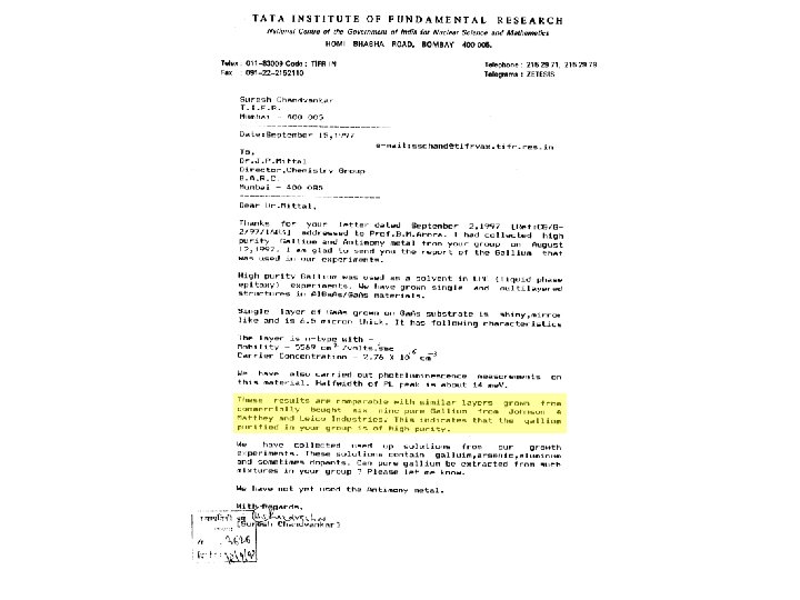
6 N Arsenic and 7 N Gallium MAT Lab, BARC Ga. As growth run Desirable Gallium arsenide single crystal SSPL, Delhi Resistivity (Ohm cm) 1. 0 - 3. 0 x 107 Mobility (cm 2/V sec) Carrier conc. (cm-3) 5000 – 6000 5 – 8 x 10⁷ Gallium and arsenic (BARC) 2. 7 x 10⁷ Tail - 5615 6. 9 x 10⁷ Gallium and arsenic (Johnson Matthey, UK) Tail – 5245 14 x 107 3. 3 x 10⁷
Purification of Indium Experimental set-up for electro-winning of vacuum fused indium Analytical data (in ppm) of purified indium metal Elemen Commercial ts Indium Vacuum fused Indium Electro-refined Indium Electrowinning indium Ag As Al Bi Cd Co Cr Cs Cu 0. 27 9. 45 9. 80 2. 17 6. 90* 24. 66 26. 70 273 3. 70 (<0. 50*) 2. 0* 3. 14 1. 85 <0. 05* 5. 06 <1. 00* 1. 77 (8. 50*) 0. 15 2. 31 5. 70 0. 52 0. 65* 8. 85 13. 97 93. 37 2. 16 (<0. 50*) <0. 5* 0. 63 1. 66 <0. 05* 1. 21 <1. 00* 1. 10 (8. 00*) 0. 88 0. 36 0. 80* 1. 62 4. 95 - 0. 03 0. 60 0. 50 0. 70* 0. 38 1. 96 - <0. 5* 0. 12 <0. 05* <0. 10* 0. 71 (<2. 00*) 5. 02 3. 63 11. 35 (11. 50*) 4. 63 0. 56 2. 70* 398. 91 0. 91 2. 16 11. 50 (<2. 00*) 1. 68 0. 26 0. 90* 157. 58 0. 91 - <0. 5* 0. 10 <0. 05* 0. 19 <0. 10* 0. 65 (<0. 200*) 0. 65 3. 62 0. 00 0. 05* 11. 05 0. 00 0. 05 0. 20* 10. 28 Fe Hg Mg Mn Mo Ni Pb Sb Se Sn Experimental set-up for electro-refining of vacuum fused indium Te Tl Zn Total * analysed by ICP-MS and remaining values from GD-QMS Chopade & Sagoria, BARC/2008/I/007
High purity antimony rods to NPCIL 7 mm diameter x 480 mm length
Zone refining (ZR) unit induction heating equipment High purity quartz tube with glassy carbon boats containing 4 -5 N germanium Busbar and induction coil unit suitable for single molten zone 12. 5 k. W, 400 KHz solid state power supply for induction unit 20 mm Bottom surface 400 mm Initial impurity concentration ~3600 ppb (<0. 001%) (~5 N) Final impurity concentration after 15 passes ~74 ppb (<0. 000001%)(~8 N) Ge crystal Wt. : ~ 800 g Orientation: <100> Ambient: Argon (6 N)
Raw Material (e. g. Si, Ga, In, As, Cd, Te) Organometallic Precursors (e. g. Trimethyl gallium, Trimehtyl Arsenic, Trimehtyl Antimony) Ultrapure Material (7 N) Vacuum Distill. , Fractional Sublim. , Electrolysis (e. g. Si, Ga, In, As, Cd, Te) Single Crystal Growth BC, CZ, VGF, ZM (e. g. Si, Ga. As , Cd. Te MOCVD Wafer Cutting/ polishing multi-wire saw, grinder, automatic polisher, etching Chip Fabrication Ion implantation, photolithography Device Integration End User
Organometallic precursors for materials synthesis Me 3 Ga + As. H 3 650 OC H 2 Ga. As + 3 Me. H H. M. Mansevit, Appl. Phy. Lett. , 12 (1968) 156)
Synthesis of Triorganogallium 2 Ga + 3 Me 2 Hg 2 Me 3 Ga + 3 Hg 2 Ga. Cl 3 + 3 Me 2 Zn 2 Me 3 Ga + 3 Zn. Cl 2 Ga. Cl 3 + 3 Me 3 Al Me 3 Ga + 3 Me 2 Al. Cl MCl 3 + 3 Me. Li MCl 3 + 3 RMg. I 2 M + 6 RMg. X Mg 5 Ga 2 + 8 RI Me 3 M + 3 Li. Cl Et 2 O THF or Et 2 O Electrolysis R 3 M. Et 2 O + 3 Mg. Cl. I 2 R 3 M. solvent + 3 Mg. X 2 2 R 3 Ga. OEt 2 + 3 Mg. I 2 + 2 Me. Mg. I (i) Adduct formation (ii) Pyrolysis of adduct (iii) Distillation R 3 Ga Jain, et. al. , BARC/2002/R/001
Electronic grade Trimethylgallium Comparison of mobility and carrier concentration of gallium arsenide layers grown with BARC TMGa and Commercial (Akzo Nobel SSG grade) TMGa (courtesy Prof. B. M. Arora, TIFR, Mumbai)
ECl 3 + 3 RMg. X As. Cl 3 + Bz. Mg. Cl R 3 E + 3 Mg. XCl Bz. As. Cl 2 + Mg. Cl 2 Bz. As. Cl 2 + 2 Me. Mg. I Bz. As. Me 2 + 2 Mg. Cl. I (E = As or Sb) [Pd 2 Me 2( -Cl)2(As. Pri 3)2] Pd. Cl 2[As(CH 2 CMe=CH 2)3]2 trans-[Pd. Cl 2(As. Pri 3)2] K. P. Chaudhari, et. al. , BARC/2003/I/004 K. P. Chaudhari, et. al. , BARC/2002/R/013 trans-[Pd. Cl 2(Sb. Pri 3)2]
Me 3 Ga + As. H 3 650 OC H 2 Ga. As + 3 Me. H
V-VI Sb 2 E 3, Bi 2 E 3 IV-VI Pb. S, Pb. Se III-VI In 2 S 3 II-VI ME (M = Zn, Cd, Hg; E = S, Se , Te) I-VI Cubic M 2 E (M = Cu, Ag, Au; E = S, Se , Te) Hexagonal
[In{Se. C 5 H 3(3 -Me)N}3] [Cu{Se. C 5 H 3(Me-3)N}]4 Cu. In. Se 2 b Thermolysis in TOPO at 330 o. C for 10 min In 2 Se 3 (103) (101) Thermolysis in TOPO (002) o at 150 C for 25 min Cu 7 Se 4 AACVD at 360 o. C for 1 h Cu 5 Se 4 250 nm Jain and co-workers, J. Organomet. Chem. , 747 (2013) 113.
[Me 2 Sn(2 -Se. C 5 H 4 N)2] [t. Bu 2 Sn(2 -Se. C 5 H 4 N)2] [Me 2 Sn{2 -Se. C 5 H 3 N(Me-3)}Cl] SEM images of Sn. Se obtained by thermolysis of [Et 2 Sn{2 -Se. C 5 H 3(Me-3)N}2] in 6 ml of oleylamine at 215 o. C for 25 min SEM image of orthorhombic Sn. Se thin film comprising of rectangular sheets deposited by AACVD of [t. Bu 2 Sn(2 Se. C 5 H 4 N)2] at 490 o. C for 3 h on a glass substrate. Photo response of the Sn. Se thin film deposited on a silicon substrate by AACVD of [t. Bu 2 Sn(2 Se. C 5 H 4 N)2] (5) at 490 o. C with a bias voltage of 1. 5 V AFM image of orthorhombic Sn. Se thin film deposited by AACVD of [t. Bu 2 Sn(2 -Se. C 5 H 4 N)2] at 530 o. C for 3 h on a glass substrate Dalton Trans. , 41 (2012) 12129
Precursors for Tin Selenide nanoparticles and thin films R 2 Sn{Se. C 4 H(4, 6 -Me)N 2}2 R 2 Sn. Cl 2 + 2 Na. Se. C 4 H(4, 6 -Me)N 2 (R = Me, Et, t. Bu) R 2 Sn. Cl 2 R 2 Sn{Se. C 4 H(4, 6 -Me)N 2}Cl t. Bu 50 nm 2 Sn{Se. C 4 H(4, 6 -Me)N 2}2 OLA 200 C, 20 min Sn. Se 2 nano-crystals XRD of Sn. Se 2 hexagonal phase 10 nm TEM and SAED pattern of hexagonal Sn. Se 2 SEM image of Sn. Se 2 thin film obtained by AACVD
[Sb{Se-C 5 H 3(Me-3)N}3]. 2 H 2 O SEM image of uniformly coated antimony selenide film obtained by AACVD of [Sb{Se. C 5 H 3(Me-3)N}3] at 425 o. C for a) 1 h and b) 2 h (Inset displays the magnified image of the same). R. K. Sharma, et. al. , Dalton Trans. 39 (2010) 8779. [Bi{Se-C 5 H 3(Me-3)N}3]. 2 H 2 O a b c d a) SEM pictures of bismuth selenide boats (Inset shows arrangement of boat like structures in a diagonally cleaved hexagon shape), b) petals, c) sheets and d) wool like structures obtained by AACVD of [Bi{Se-C 5 H 3(Me-3)N}3] at 350, 375, 400 and 475 o. C, respectively for 1 h.
Inorganic Materials System Examples No. of possible system Reported so far Unitary Si, Ge 100 (100%) Binary Cd. Se, Ga. As 4950 4000 (~80%) Ternary Cu. In. Se 2, Hg. Cd. Te 1, 61, 700 8000 (~5%) Quaternary Cu. Ga. In. S 2, Ga. In. PAs 39, 21, 225 1000 (<0. 05%) P. Wu et. al. , Chem. Mater. , 12 (2000) 1648
Duration In-Charge Activities 1957 -1961 Dr. N. S. K. Prasad U, Nb, Si 1961 -1985 Dr. G. S. Rao Nuclear materials, rare earth compounds Primary materials for semiconductor technology (Ag, Zn, Cd, Ga, In, Sn, Pb, P, As, Sb, Bi, Se, Te, Al. N, POCl 3, POBr 3, PBr 3) (Know-how to NFC transferred) Zone refining Na. I scintillator Ga. P, Ga. As, Cd. Se, Zn. S, Cd. S Ga technology transferred to Hindalco 1986 -1994 Dr. A. J. Singh Ca. SO 4. Dy 2(SO 4)3 (TLD Phosphor) BN, high Tc superconductors, etc. MASCOT project, Ga, As 1995 -1999 Dr. T. K. Das MASCOT Project , Ga, As 1999 -2000 Dr. G. M. Phatak MASCOT Project , Ga, As 2000 -till date Dr. V. K. Jain MASCOT Project , ultra-purification of Ga and As Design and development of organometallic precursors for advanced materials Sankofa Bird Dr. J. P. Mittal Dr. T. Mukherjee Dr. S. K. Sarkar Dr. B. N. Jagatap Dr. D. Das Shri K. Gangadharan Shri. K. B. Bhatt Shri V. S. Sagoria Shri Kamal Choudhary Shri S. M. Chopade Smt. Nisha Kushwaha Smt. Alpa Shah Shri Amey Wadawale Shri Manoj K. Pal Dr. Sandip Dey Dr. L. B. Kumbhare Dr. G. Kedarnath Dr. P. P. Phadnis Shri Adish Tyagi Ph. D. Students
Excellence ↔ Relevance Development- Demonstration Deployment (RD 3) Technology What next? molecules materials machines Mission make in India