Pierpaolo Valerio DESIGN CONSIDERATIONS FOR CLICPIX 2 AND


- Slides: 15

Pierpaolo Valerio DESIGN CONSIDERATIONS FOR CLICPIX 2 AND STATUS REPORT ON THE TSV PROJECT 1

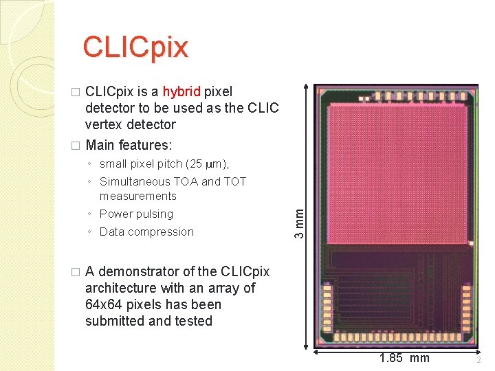
CLICpix is a hybrid pixel detector to be used as the CLIC vertex detector � Main features: � ◦ Simultaneous TOA and TOT measurements ◦ Power pulsing ◦ Data compression � 3 mm ◦ small pixel pitch (25 μm), A demonstrator of the CLICpix architecture with an array of 64 x 64 pixels has been submitted and tested 1. 85 mm 2

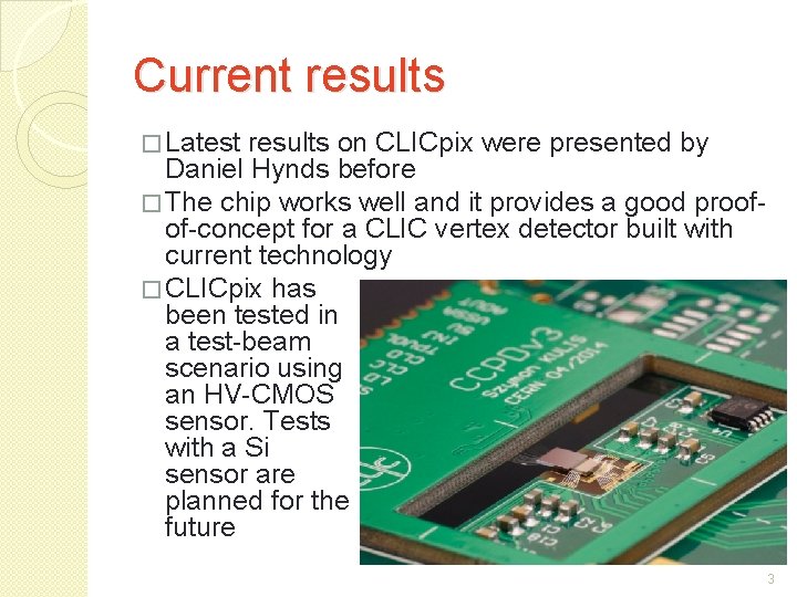
Current results � Latest results on CLICpix were presented by Daniel Hynds before � The chip works well and it provides a good proofof-concept for a CLIC vertex detector built with current technology � CLICpix has been tested in a test-beam scenario using an HV-CMOS sensor. Tests with a Si sensor are planned for the future 3

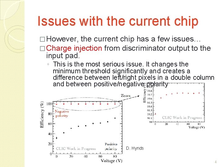
Issues with the current chip � However, the current chip has a few issues… � Charge injection from discriminator output to the input pad. ◦ This is the most serious issue. It changes the minimum threshold significantly and creates a difference between left/right pixels in a double column and between positive/negative polarity D. Hynds 4

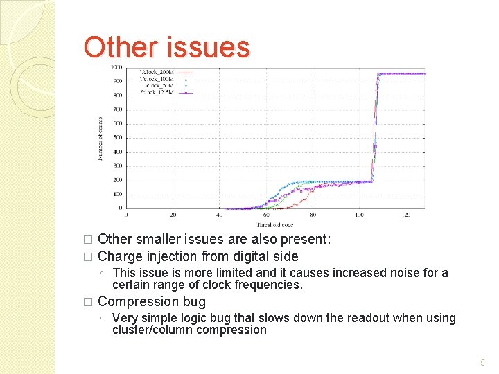
Other issues Other smaller issues are also present: � Charge injection from digital side � ◦ This issue is more limited and it causes increased noise for a certain range of clock frequencies. � Compression bug ◦ Very simple logic bug that slows down the readout when using cluster/column compression 5

Design limitations �Small counters ◦ 4 bits TOA is not enough (even for a CLIC application) �We require a 10 ns accuracy over a 160 ns period, so we need 5 bits to accommodate for chip-to-chip timing calibration ◦ 4 bits TOT is enough, but a longer counter would allow more accurate measurements ◦ 4 bits event counter results in really long and tedious testing routines �Small matrix (64 by 64 pixels) ◦ Small area increases the time it takes to get statistics �“Clunky” readout ◦ A few interface design choices resulted in a more complicated test setup than what was foreseen 6

CLICpix 2: Architecture improvements �Larger Counters ◦ 6 bits TOT for more accurate energy measurements ◦ 8 bits TOA should be possible – a total of 14 bits is most probably achievable, but it needs to be validated ◦ A new mode of operation with a single 14 bits counter for To. A / Event Counting �Larger matrix (128 by 128) �More convenient readout ◦ 8/10 bit encoding for high speed readout �A few more IP blocks can be used (and tested), such as a band-gap 7

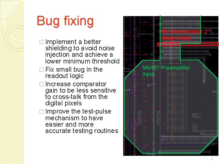
Bug fixing � Implement a better shielding to avoid noise injection and achieve a lower minimum threshold � Fix small bug in the readout logic � Increase comparator gain to be less sensitive to cross-talk from the digital pixels � Improve the test-pulse mechanism to have easier and more accurate testing routines M 4 Discriminator 2 nd stage output M 6/M 7 Preamplifier input 8

Project status �The analog part of the pixel was updated and re-simulated successfully ◦ This part needs to be laid out again from scratch to merge structures among adjacent pixels and to reduce cross-talk �The digital pixel part was modified and fixed. However, a more robust testbench for the digital side is required to avoid bugs �IP blocks need to be integrated �Periphery blocks must be updated to correctly manage the larger pixel matrix 9

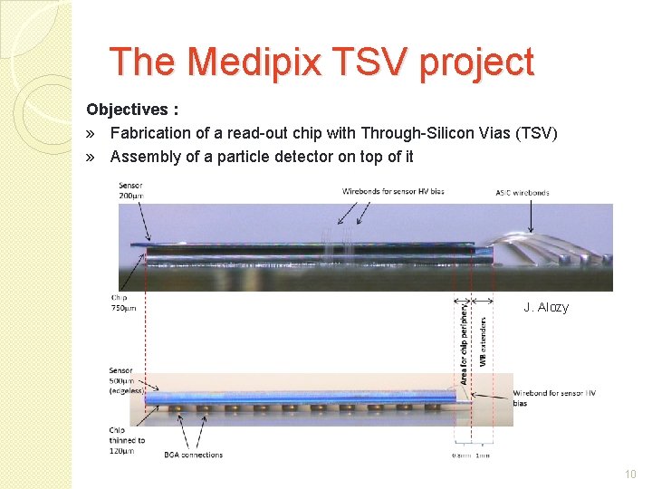
The Medipix TSV project Objectives : » Fabrication of a read-out chip with Through-Silicon Vias (TSV) » Assembly of a particle detector on top of it J. Alozy 10

TSV second run � Launched in CEA LETI (Grenoble) in March 2014 and delivered to CERN in October 2014 ◦ The main motivation of the second run was to obtain good yields in order to validate the TSV process applied on Medipix chips � Lot # μSA 999 P of 3 wafers: ◦ P 04 (W 128 -AZPGBPH) : completed, delivered to CERN and tested ◦ 14 chips (7 class AA + 7 with other classes) sent to ADVACAM for assembly First assemblies recently received. Test in progress. ◦ P 05 (W 127 -AKPGALH) : need rework (during 3 D 06) ◦ P 06 (W 126 -AMPG 6 LH) : completed, delivered to CERN and tested � Lot # μSB 254 P of 3 wafers ◦ P 01 (W 125 A 3 PGC 2 H) : completed, delivered to CERN and tested ◦ P 02 (W 124 ACPGAUH) : completed, delivered to CERN and tested ◦ P 03 (W 123 A 0 PGBNH) : completed, delivered to CERN and 11

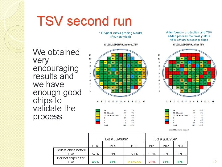
TSV second run After foundry production and TSV added process the final yield is 45% of fully functional chips * Original wafer probing results (Foundry yield) We obtained very encouraging results and we have enough good chips to validate the process Lot # μSA 999 P Perfect chips before TSV Perfect chips after TSV Lot # μSB 254 P P 04 P 05 P 06 P 01 P 02 P 03 57% 51% 50% 60% 53% 45% 41% In rework 20% 41% 38% 12

TSV third run �LOT 1: stopped with TSV-last seed deposition due to presence of residues in via bottom ◦ estimated delivery date: moved from mid November 14 to February 2015 �LOT 2: at TSV etching, stopped until polymer issue is solved ◦ LOT 2 estimated delivery date: moved from end of December 14 to march 2015 13

TSV third run � Some arcing effects at wafer edge were observed after hard mask etching ◦ Arcing issue is a well know problem with silicon on “spin on glass” wafers due to capacitive effect of substrate on electrostatic chuck ◦ Problem has been fixed on 120 µm thick wafers (no issue on last run) With 50 µm wafers the capacitance increases and makes the process more sensitive � The issues are more important because of the presence of defects at the edge of the wafer : glue or lithography resin residues. No arcing on Si test wafers � These defects are limited to the very edges of the wafer an good dies should not be affected � � Polymer residues were observed at TSV bottom after RDL lithography step of LOT#1. It has been decided to stop the process to try to remove the residues and investigate how to avoid this effect on LOT#2 14

THANKS FOR YOUR ATTENTION Your input for CLICpix 2 is welcome!! 15