CLICpix 2 Design Status Pierpaolo Valerio and Edinei




- Slides: 34

CLICpix 2 Design Status Pierpaolo Valerio and Edinei Santin CLICdp Vertex Meeting - August 12 th 2015

Digital Design Part Pierpaolo Valerio

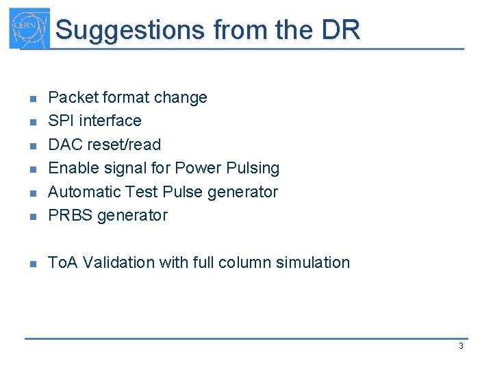
Suggestions from the DR n Packet format change SPI interface DAC reset/read Enable signal for Power Pulsing Automatic Test Pulse generator PRBS generator n To. A Validation with full column simulation n n 3

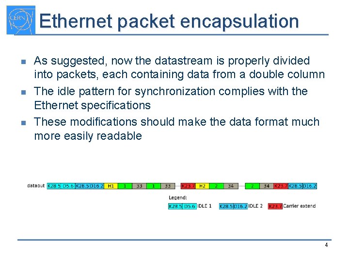
Ethernet packet encapsulation n As suggested, now the datastream is properly divided into packets, each containing data from a double column The idle pattern for synchronization complies with the Ethernet specifications These modifications should make the data format much more easily readable 4

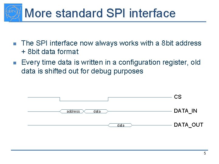
More standard SPI interface n n The SPI interface now always works with a 8 bit address + 8 bit data format Every time data is written in a configuration register, old data is shifted out for debug purposes CS address DATA_IN data DATA_OUT 5

New programming algorithm n Using the SPI interface, matrix programming is now done using a standard command, 8 bits at a time n This makes implementing the DAQ firmware easier, but it comes at the cost of additional overhead when performing the programming routine 6

PRBS for link testing n n n There is now a command to have the chip send a sequence of pseudo-random data to test the error rate of the link between the chip and the DAQ The same command stops the data stream The sequence is periodic with a very long period (65 k words) 7

Automatic Test-Pulse generator n n n The chip can now be programmed to generate a sequence of test pulses automatically Both the number of pulses and the delay between them can be programmed independently; enough test pulses can be produced to saturate the 13 -bit event counter It is still possible to use an external trigger if needed 8

Other features n n DACs are now reset at the nominal values when the global reset signal is asserted It is possible to disable the power pulsing with a configuration option q The power pulsing logic will still be used, but the biasing lines will not be switched 9

Full column To. A simulation n A full column was simulated with a fully extracted digital model and a simplified analog model to check for the validity of the To. A measurements The analog pixel has “realistic” noise and mismatch models Sending a pulse to all pixels at the same time, the expected behavior is to have two different To. A results (due to the unknown phase of the input pulse related to the clock) 10

Full column To. A simulation n 1000 test pulses were injected with random arrival and shutter times in the simulation Without noise and mismatch the To. A had no errors (only two values are recorded) With noise and mismatch, we have an error rate of ~0. 013% 11

Things left to do n n Check the feasibility of the fastor signal Code cleanup q n n Some minor suggestions made during the code review need to be implemented Simulation of the interface with the DAQ Placing DDR buffer Synthesis of the periphery Simulation of extracted periphery + pixel matrix 12

Analog Design Part Edinei Santin

DR points covered here n n Further verification of the frontend in terms of PSRR and stability/noise wrt to leakage current and input capacitance Verification of the output swing of the comparator New topology for the calibration DAC Crosstalk between pixels 14

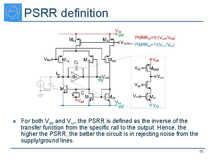
PSRR definition n For both Vdd and Vss, the PSRR is defined as the inverse of the transfer function from the specific rail to the output. Hence, the higher the PSRR, the better the circuit is in rejecting noise from the supply/ground lines. 15

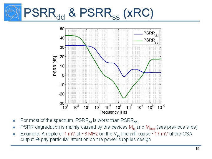
PSRRdd & PSRRss (x. RC) n n n For most of the spectrum, PSRRss is worst than PSRRdd PSRR degradation is mainly caused by the devices Min and Mload (see previous slide) Example: A ripple of 1 m. V at ~3 MHz on the Vss line will cause ~17 m. V at the CSA output pay particular attention on the power supplies design 16

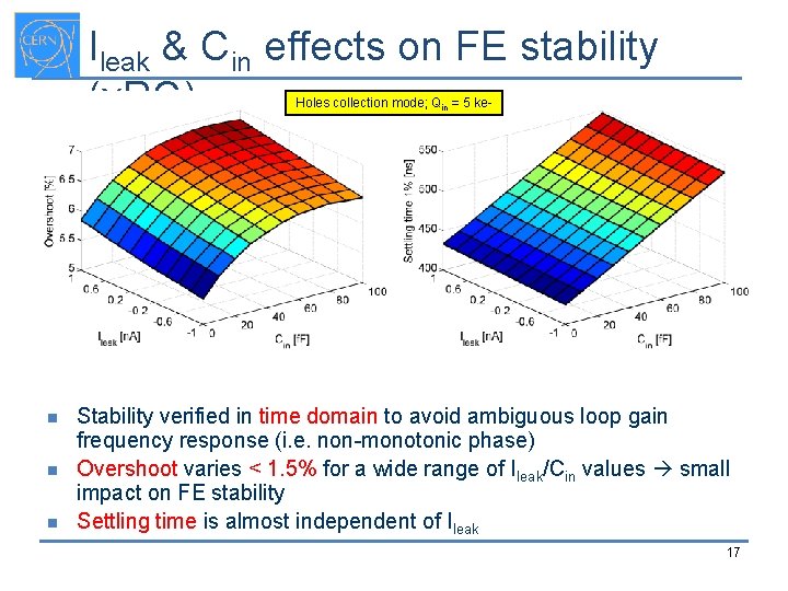
Ileak & Cin effects on FE stability (x. RC) Holes collection mode; Qin = 5 ke- n n n Stability verified in time domain to avoid ambiguous loop gain frequency response (i. e. non-monotonic phase) Overshoot varies < 1. 5% for a wide range of Ileak/Cin values small impact on FE stability Settling time is almost independent of Ileak 17

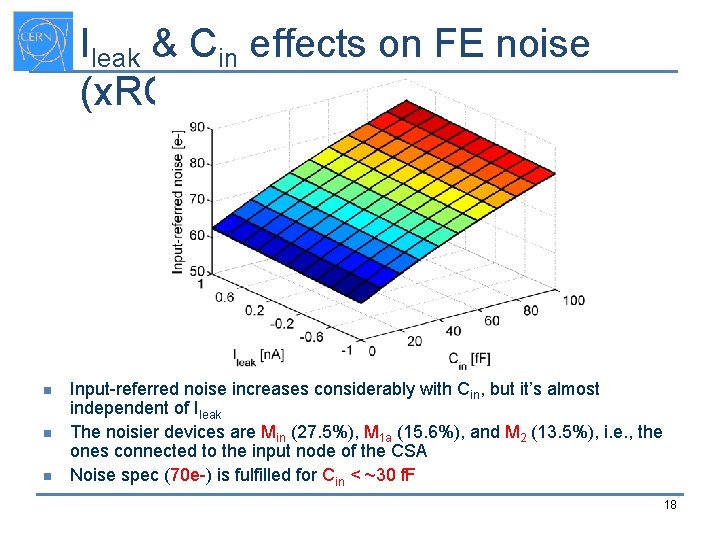
Ileak & Cin effects on FE noise (x. RC) n n n Input-referred noise increases considerably with Cin, but it’s almost independent of Ileak The noisier devices are Min (27. 5%), M 1 a (15. 6%), and M 2 (13. 5%), i. e. , the ones connected to the input node of the CSA Noise spec (70 e-) is fulfilled for Cin < ~30 f. F 18

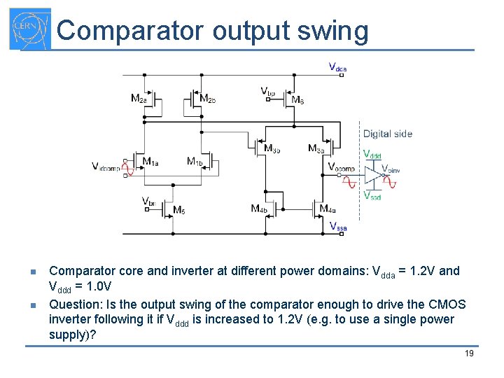
Comparator output swing n n Comparator core and inverter at different power domains: Vdda = 1. 2 V and Vddd = 1. 0 V Question: Is the output swing of the comparator enough to drive the CMOS inverter following it if Vddd is increased to 1. 2 V (e. g. to use a single power supply)? 19

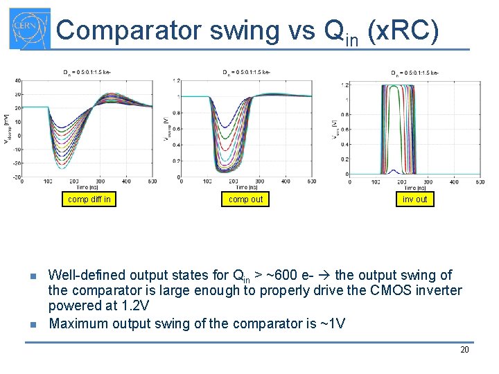
Comparator swing vs Qin (x. RC) comp diff in n n comp out inv out Well-defined output states for Qin > ~600 e- the output swing of the comparator is large enough to properly drive the CMOS inverter powered at 1. 2 V Maximum output swing of the comparator is ~1 V 20

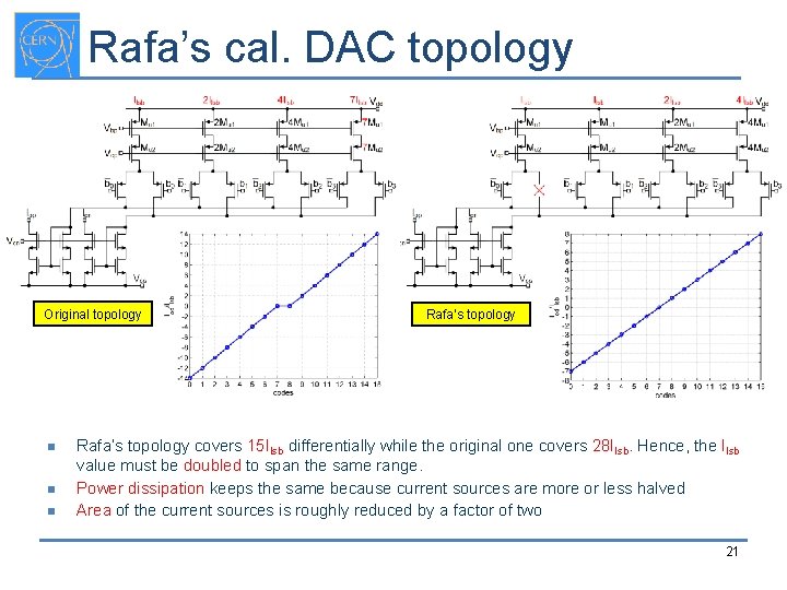
Rafa’s cal. DAC topology Original topology n n n Rafa’s topology covers 15 Ilsb differentially while the original one covers 28 Ilsb. Hence, the Ilsb value must be doubled to span the same range. Power dissipation keeps the same because current sources are more or less halved Area of the current sources is roughly reduced by a factor of two 21

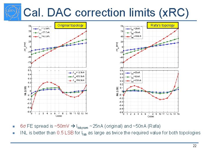
Cal. DAC correction limits (x. RC) Original topology n n Rafa’s topology 6σ FE spread is ~50 m. V Ilsb, nom ~25 n. A (original) and ~50 n. A (Rafa) INL is better than 0. 5 LSB for Ilsb as large as twice the required value for both topologies 22

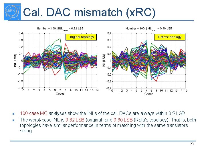
Cal. DAC mismatch (x. RC) Original topology n n Rafa’s topology 100 -case MC analyses show the INLs of the cal. DACs are always within 0. 5 LSB The worst-case INL is 0. 32 LSB (original) and 0. 30 LSB (Rafa’s topology). That is, both topologies have similar performance in terms of matching with the same transistors sizing 23

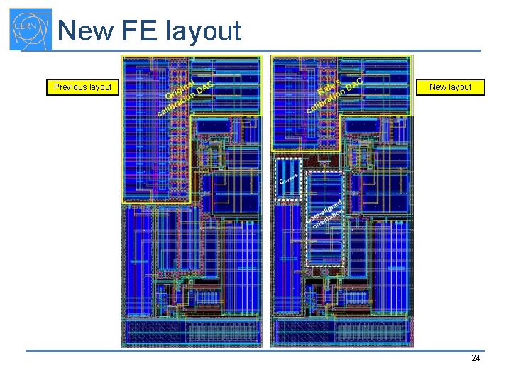
New FE layout Previous layout New layout 24

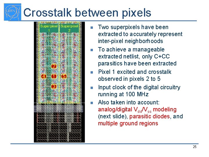
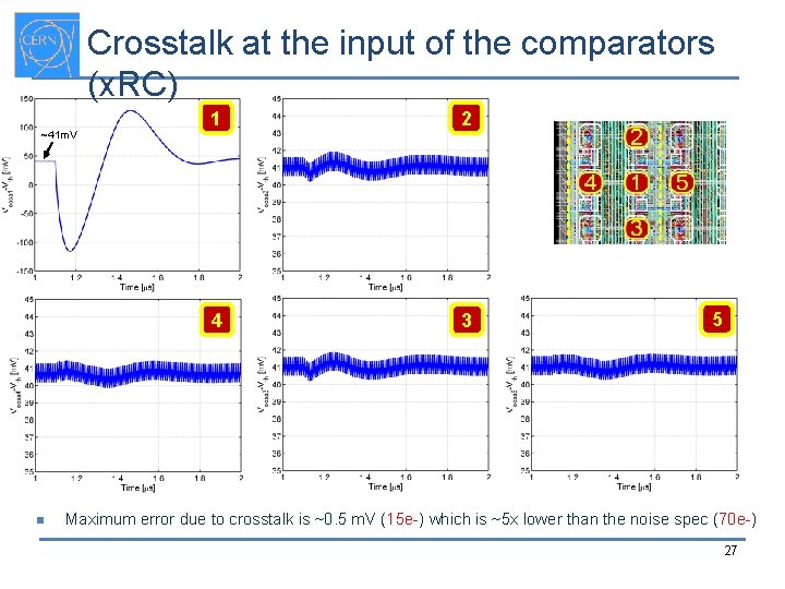
Crosstalk between pixels n n n Two superpixels have been extracted to accurately represent inter-pixel neighborhoods To achieve a manageable extracted netlist, only C+CC parasitics have been extracted Pixel 1 excited and crosstalk observed in pixels 2 to 5 Input clock of the digital circuitry running at 100 MHz Also taken into account: analog/digital Vdd/Vss modeling (next slide), parasitic diodes, and multiple ground regions 25

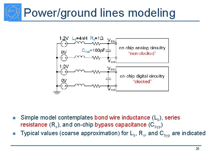
Power/ground lines modeling n n Simple model contemplates bond wire inductance (Lb), series resistance (Rs), and on-chip bypass capacitance (Cbyp) Typical values (coarse approximation) for Lb, Rs, and Cbyp are indicated 26

Crosstalk at the input of the comparators (x. RC) ~41 m. V n 1 2 4 3 5 Maximum error due to crosstalk is ~0. 5 m. V (15 e-) which is ~5 x lower than the noise spec (70 e-) 27

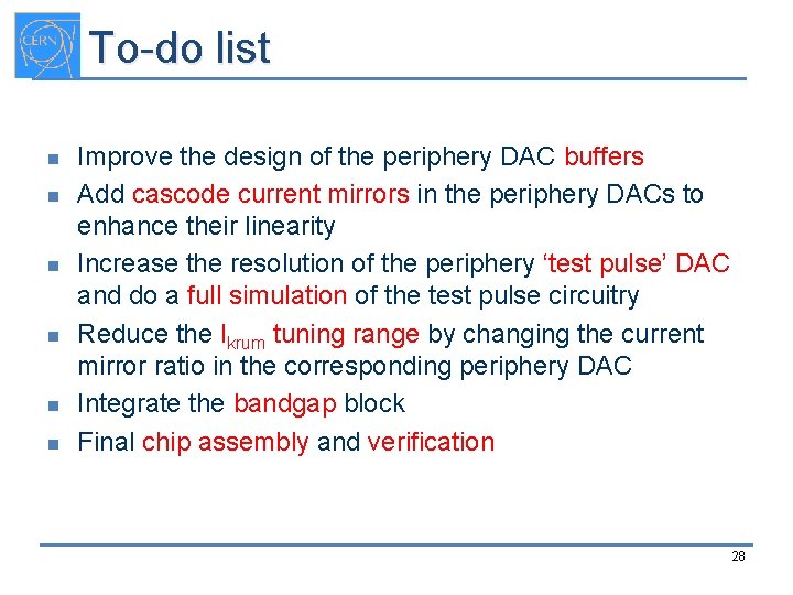
To-do list n n n Improve the design of the periphery DAC buffers Add cascode current mirrors in the periphery DACs to enhance their linearity Increase the resolution of the periphery ‘test pulse’ DAC and do a full simulation of the test pulse circuitry Reduce the Ikrum tuning range by changing the current mirror ratio in the corresponding periphery DAC Integrate the bandgap block Final chip assembly and verification 28

Thank you!

Backup slides

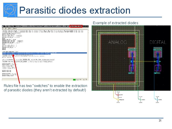
Parasitic diodes extraction Example of extracted diodes Rules file has two “switches” to enable the extraction of parasitic diodes (they aren’t extracted by default!) 31

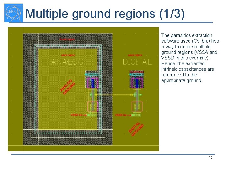
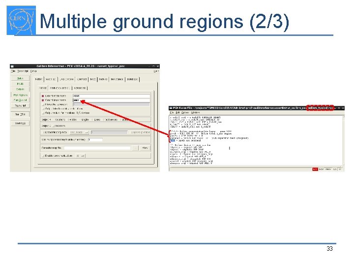
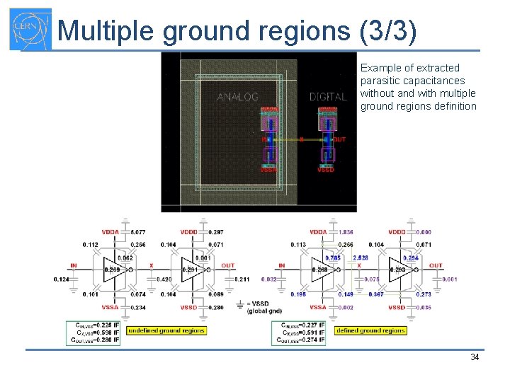
Multiple ground regions (1/3) The parasitics extraction software used (Calibre) has a way to define multiple ground regions (VSSA and VSSD in this example). Hence, the extracted intrinsic capacitances are referenced to the appropriate ground. 32

Multiple ground regions (2/3) 33

Multiple ground regions (3/3) Example of extracted parasitic capacitances without and with multiple ground regions definition 34