Preliminary testing results on the CLICpix demonstrator Szymon
- Slides: 13

Preliminary testing results on the CLICpix demonstrator Szymon Kulis and Pierpaolo Valerio

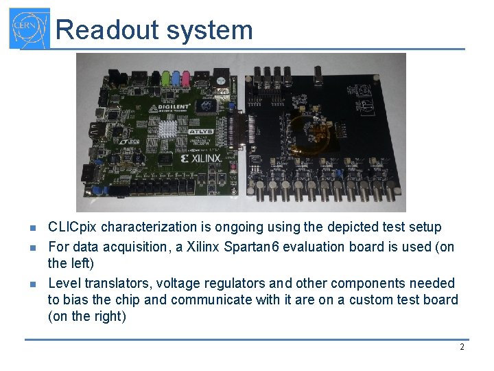
Readout system n n n CLICpix characterization is ongoing using the depicted test setup For data acquisition, a Xilinx Spartan 6 evaluation board is used (on the left) Level translators, voltage regulators and other components needed to bias the chip and communicate with it are on a custom test board (on the right) 2

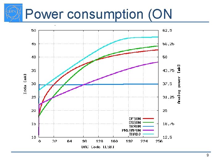
First tests n n n Preliminary tests on the custom PCB were positive, with only minor issues which can be easily fixed The chip is alive and measurements on global power consumption are consisted with what we expected The chip reads commands from the FPGA and answers accordingly 3

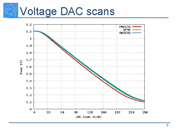
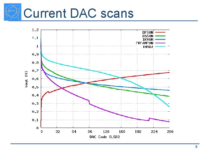
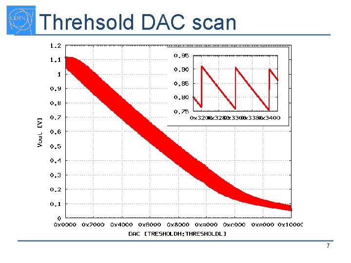
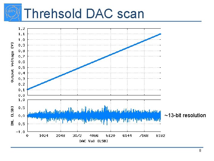
Periphery DAC characterization n n The chip correctly interpreted the commands to program the periphery DACs, so DAC scans could be performed (measuring their output with a multimeter) All measured DACs perform according to simulations, within uncertainty due to process variations. Voltage DACs show a good linearity in the 0. 15 V – 1 V range, where they are supposed to operate 4

Voltage DAC scans 5

Current DAC scans 6

Threhsold DAC scan (uncorrected) 7

Threhsold DAC scan (corrected) ~13 -bit resolution 8

Power consumption (ON state) 9

Pixel matrix digital tests n n n The pixel matrix can be programmed with configuration data and verified correctly Pixel configuration data influence analog pixel behaviour according to expectations (test pulse, threshold adjustment DAC, polarity bit) Non-compressed readout of random strings was tested and found to be working correctly 10

Preliminary analog observation n n Despite some difficulties in the measurment process, the analog pixel is functionally working (test pulses are injected, shaped and discriminated according to the chip programming) Power pulsing capabilities have the expected impact on the matrix analog power consumption 11

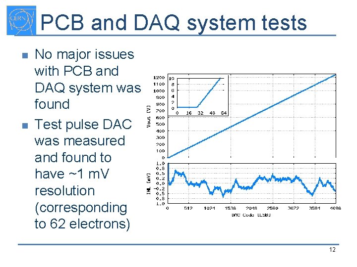
PCB and DAQ system tests n n No major issues with PCB and DAQ system was found Test pulse DAC was measured and found to have ~1 m. V resolution (corresponding to 62 electrons) 12

Conclusions and next steps n n n No major bugs were found (till now) All measurements correspond to simulations within expected uncertainties Next measurements include q q q trying to perform more accurate measurements on the analog front-end perform a complete acquisition using test pulses perform power pulsing timing measurements 13