Pelican IP Pictures Com LSI Inc Confidential and
- Slides: 19

Pelican IP Pictures Com. LSI Inc. Confidential and Proprietary information 12/12/2006 Confidential / Proprietary

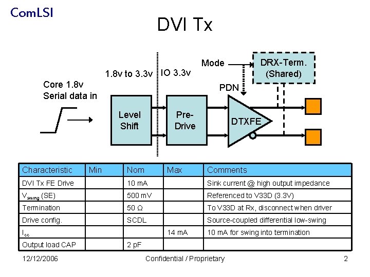
Com. LSI DVI Tx 1. 8 v to 3. 3 v IO 3. 3 v Core 1. 8 v Serial data in PDN Level Shift Characteristic Min DRX-Term. (Shared) Mode Pre. Drive Nom Max DTXFE Comments DVI Tx FE Drive 10 m. A Sink current @ high output impedance Vswing (SE) 500 m. V Referenced to V 33 D (3. 3 V) Termination 50 Ω To V 33 D at Rx, disconnect when driver Drive config. SCDL Source-coupled differential low-swing Icc Output load CAP 12/12/2006 14 m. A 10 m. A for swing into termination 2 p. F Confidential / Proprietary 2

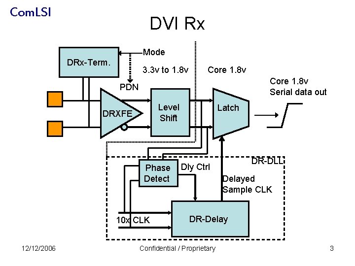
Com. LSI DVI Rx Mode DRx-Term. 3. 3 v to 1. 8 v Core 1. 8 v Serial data out PDN Level Shift DRXFE Phase Detect 10 x CLK 12/12/2006 Latch DR-DLL Dly Ctrl Delayed Sample CLK DR-Delay Confidential / Proprietary 3

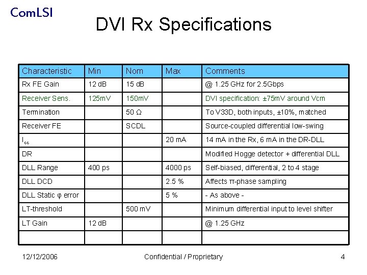
Com. LSI DVI Rx Specifications Characteristic Min Nom Max Rx FE Gain 12 d. B 15 d. B @ 1. 25 GHz for 2. 5 Gbps Receiver Sens. 125 m. V 150 m. V DVI specification: ± 75 m. V around Vcm Termination 50 Ω To V 33 D, both inputs, ± 10%, matched Receiver FE SCDL Source-coupled differential low-swing Icc 20 m. A DR DLL Range Comments 14 m. A in the Rx, 6 m. A in the DR-DLL Modified Hogge detector + differential DLL 400 ps 4000 ps Self-biased, differential, 2 to 4 stage DLL DCD 2. 5 % Affects π-phase sampling DLL Static φ error 5% - As above - LT-threshold LT Gain 12/12/2006 500 m. V 12 d. B Minimum differential input to level shifter @ 1. 25 GHz Confidential / Proprietary 4

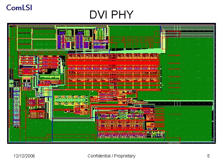
Com. LSI 12/12/2006 DVI PHY Confidential / Proprietary 5

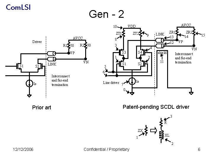
Com. LSI Gen - 2 ZT 1 AVCC Driver R 1 50 AVCC VDD 10 8 R 2 50 12 3 4 S 3 VP S 4 1 S 2 LINK Is Interconnect and far-end termination VN 5 6 Line driver S 2 15 VP VN Interconnect and far-end termination shield 2 S 1 ZR 2 14 ZR 1 13 LINK 9 11 Is 7 0 Prior art Patent-pending SCDL driver 3 R ZX 1 XL 2 12/12/2006 Confidential / Proprietary 6

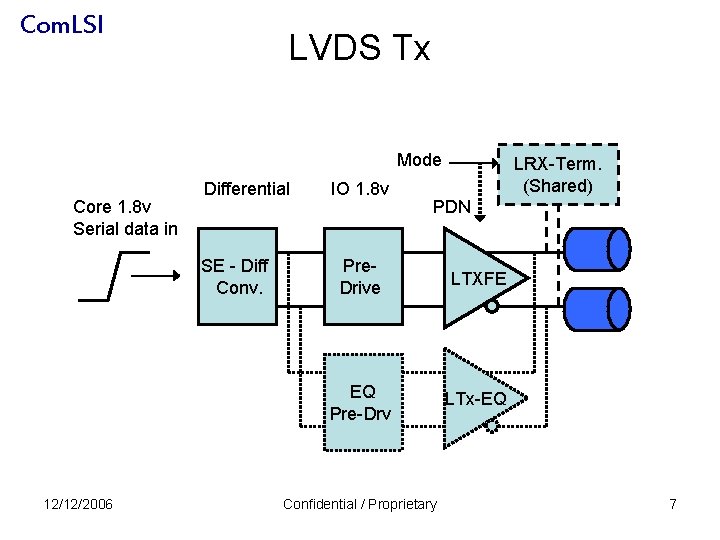
Com. LSI LVDS Tx Mode Core 1. 8 v Serial data in Differential SE - Diff Conv. 12/12/2006 IO 1. 8 v LRX-Term. (Shared) PDN Pre. Drive LTXFE EQ Pre-Drv LTx-EQ Confidential / Proprietary 7

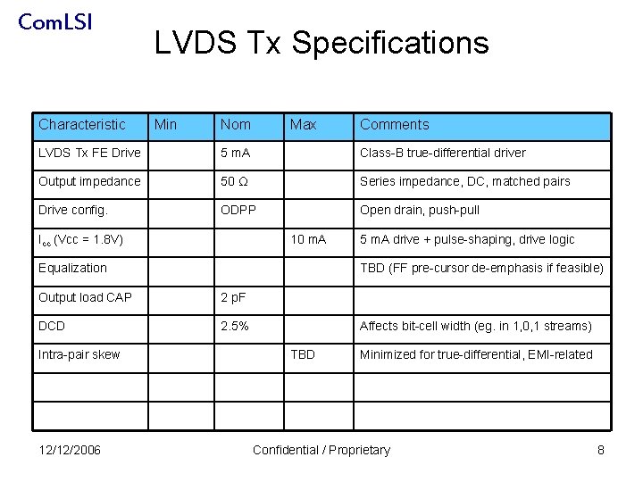
Com. LSI Characteristic LVDS Tx Specifications Min Nom Max Comments LVDS Tx FE Drive 5 m. A Class-B true-differential driver Output impedance 50 Ω Series impedance, DC, matched pairs Drive config. ODPP Open drain, push-pull Icc (Vcc = 1. 8 V) 10 m. A Equalization TBD (FF pre-cursor de-emphasis if feasible) Output load CAP 2 p. F DCD 2. 5% Intra-pair skew 12/12/2006 5 m. A drive + pulse-shaping, drive logic Affects bit-cell width (eg. in 1, 0, 1 streams) TBD Minimized for true-differential, EMI-related Confidential / Proprietary 8

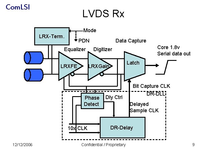
Com. LSI LVDS Rx Mode LRX-Term. PDN Equalizer LRXFE Data Capture Core 1. 8 v Serial data out Digitizer Latch LRXGain Bit Capture CLK Phase Detect 10 x CLK 12/12/2006 DR-DLL Dly Ctrl Delayed Sample CLK DR-Delay Confidential / Proprietary 9

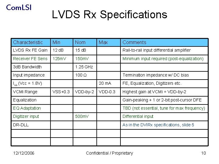
Com. LSI LVDS Rx Specifications Characteristic Min Nom Max LVDS Rx FE Gain 12 d. B 15 d. B Rail-to-rail input differential amplifier Receiver FE Sens 125 m. V 150 m. V Minimum input required (post-equalization) 3 d. B Bandwidth 1. 25 GHz Input impedance 100 Ω Icc (Vcc = 1. 8 V) VCMi Range VSS+0. 3 VDD-by-2 Comments Termination impedance w/ DC bias 20 m. A FE, Equalization, Digitizers etc. VDD-0. 3 Highest gain at VCMi = VDD-by-2 Equalization Gain-peaking + 1 or 2 -bit post-cursor DFE EQ Adaptation TBD (not essential, tune for max frequency) Digitizer input DR-DLL 12/12/2006 500 m. V Differential input As in the DVIRx specifications, slide 5 Confidential / Proprietary 10

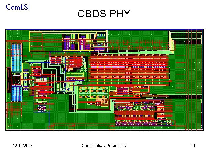
Com. LSI 12/12/2006 CBDS PHY Confidential / Proprietary 11

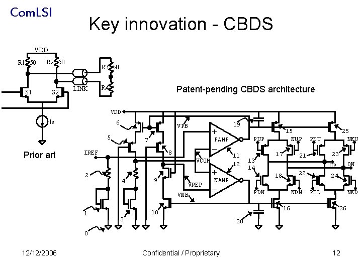
Com. LSI Key innovation - CBDS VDD R 1 50 R 2 50 S 1 S 2 R 3 50 LINK Patent-pending CBDS architecture R 4 VDD Is 6 VPB 5 Prior art + – 8 VCOM 4 9 + VREP VNB 1 11 12 13 14 17 – 23 ON OP 22 PDN NDN 16 10 25 NEU PEU 21 18 NAMP 3 15 NUP PAMP 7 IREF 2 19 24 PED NED 26 20 0 12/12/2006 Confidential / Proprietary 12

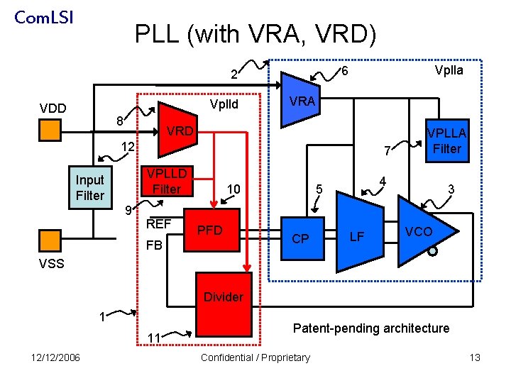
Com. LSI PLL (with VRA, VRD) Vplld VDD 8 Vplla 6 2 VRA VRD 12 7 VPLLD Filter Input Filter 9 REF 10 PFD FB 4 5 CP VPLLA Filter LF 3 VCO VSS Divider 1 11 12/12/2006 Patent-pending architecture Confidential / Proprietary 13

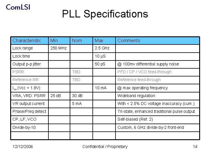
Com. LSI PLL Specifications Characteristic Min Lock range 250 MHz Nom Max Comments 2. 5 GHz Lock time 10 µS Output p-p jitter 50 p. S @ 100 mv differential supply noise PSRR TBD PFD / CP / VCO feed-through Reference RR TBD Reference feed-through Icc (Vcc = 1. 8 V) VRA, VRD: PSRR VR output current 10 m. A 25 d. B @ max operating frequency 30 d. B Wideband regulation 5 m. A With < 2. 5% DC voltage inaccuracy (cum. ) Phase/Freq detect Tri-state, enhanced traditional pulse output CP, LF, VCO Self-biased (Ref. 2) Divide-by-10 Custom, 6 GHz divide-by-2 front-end 12/12/2006 Confidential / Proprietary 14

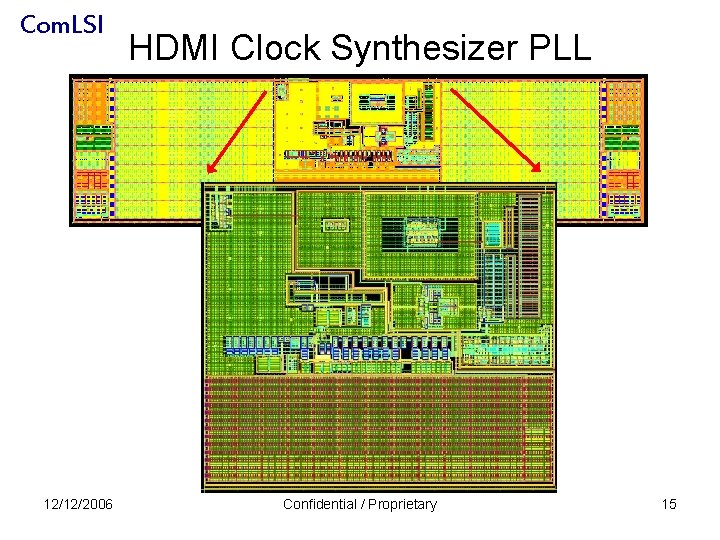
Com. LSI 12/12/2006 HDMI Clock Synthesizer PLL Confidential / Proprietary 15

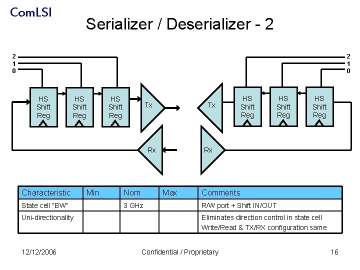
Com. LSI Serializer / Deserializer - 2 2 1 0 HS Shift Reg Tx Tx Rx Characteristic State cell “BW” Uni-directionality 12/12/2006 Min Nom HS Shift Reg Rx Max 3 GHz HS Shift Reg Comments R/W port + Shift IN/OUT Eliminates direction control in state cell Write/Read & TX/RX configuration same Confidential / Proprietary 16

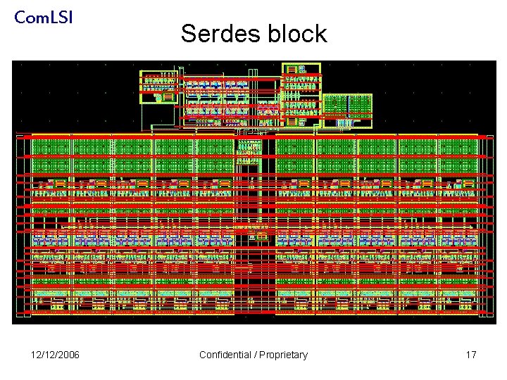
Com. LSI 12/12/2006 Serdes block Confidential / Proprietary 17

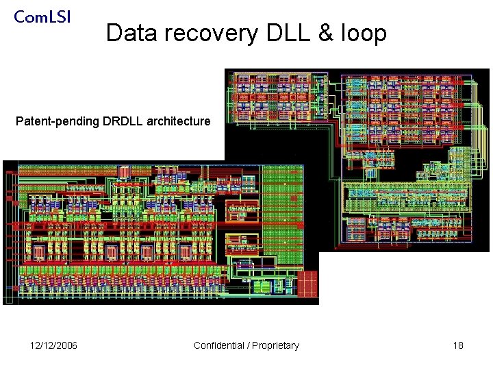
Com. LSI Data recovery DLL & loop Patent-pending DRDLL architecture 12/12/2006 Confidential / Proprietary 18

Com. LSI References 1. DVI_10. PDF: Digital Visual Interface Revision 1. 0. 02 April 1999 2. Hogge Jr. , Charles R. , “A Self Correcting Clock Recovery Circuit”, IEEE Journal of Lightwave Technology, vol. LT-3, pp. 1312 -1314, December 1985 3. Maneatis, John G. , “Low-jitter process-independent DLL and PLL based on self-biased techniques”, ISSCC 199 Dig. Tech. Papers, Feb. 1996, pp. 130 -131 4. Balan, Vishnu et al, “A 4. 8 -6. 4 -Gb/s Serial Link for Backplane Applications Using Decision Feedback Equalization”, IEEE Journal of Solid-State Circuits, Vol. 40, No. 9, September 2005 5. Sorna, M. et al, “A 6. 4 Gb/s CMOS Ser. Des Core with Feedforward and Decision-Feedback Equalization”, 2005 IEEE International Solid-State Circuits Conference 6. Razavi, B. , “Monolithic phase-locked loops and clock recovery circuits Theory and Design”, IEEE Press 1996 7. Gai, Weixin et al, “A 4 -Channel 3. 125 Gb/s/ch CMOS Transceiver with 30 d. B Equalization”, 2004 Symp. On VLSI Circuits Digest of Tech. Papers, pp. 138 -141 8. Zerbe, Jared L. et al, “Equalization and Clock Recovery for a 2. 5 -10 -Gb/s 2 -PAM/4 -PAM Backplane Trasceiver Cell”, IEEE Journal of Solid-State Circuits, Vol. 38, No. 12, Dec. 2003 9. Rahman, H. and Islam, Syed K. , “Fully-differential, high-speed current-mode controlled dividers designed using modular approach”, Internet document (publication unknown) 10. Lee, Chang-Hyeon et al, “Design of Low Jitter PLL for Clock Generator with Supply Noise Insensitive VCO”, IEEE, 1998 11. Hannah, Eric C. , “Method and apparatus to transmit signals over a cable”, US Patent 6, 452, 975 Sep. 17, 2002 12. Bazes, et al, “Adaptive equalization using a minimum-jitter method”, US Patent 5, 991, 339 Nov. 23, 1999 13. Henning Braunisch and Raj Nair, “On the Techniques of Clock Extraction and Oversampling” 12/12/2006 Confidential / Proprietary 19