NANDNAND and NORNOR Circuits and Even and Odd
- Slides: 18

NAND-NAND and NOR-NOR Circuits and Even and Odd Logic Functions

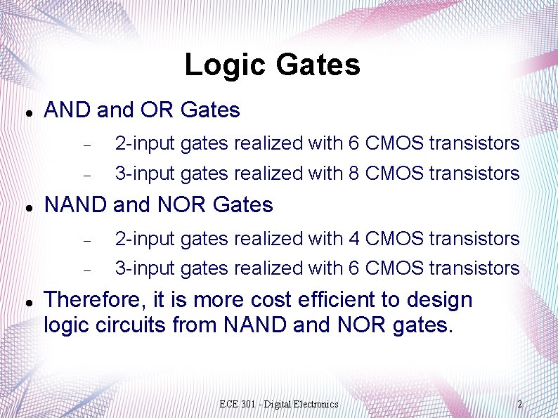
Logic Gates AND and OR Gates 2 -input gates realized with 6 CMOS transistors 3 -input gates realized with 8 CMOS transistors NAND and NOR Gates 2 -input gates realized with 4 CMOS transistors 3 -input gates realized with 6 CMOS transistors Therefore, it is more cost efficient to design logic circuits from NAND and NOR gates. ECE 301 - Digital Electronics 2

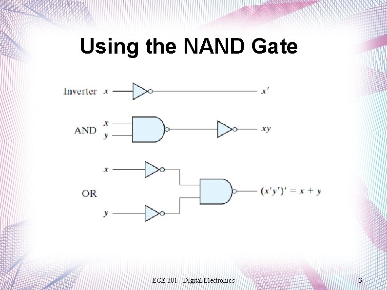
Using the NAND Gate ECE 301 - Digital Electronics 3

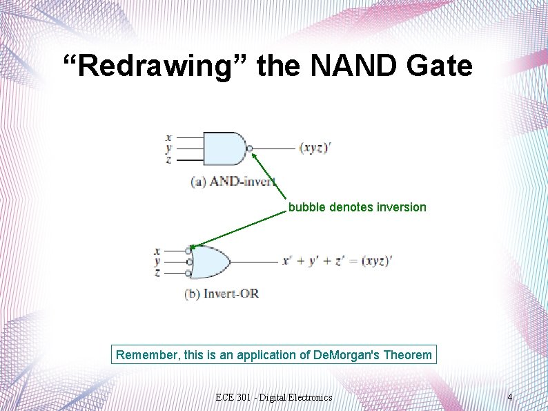
“Redrawing” the NAND Gate bubble denotes inversion Remember, this is an application of De. Morgan's Theorem ECE 301 - Digital Electronics 4

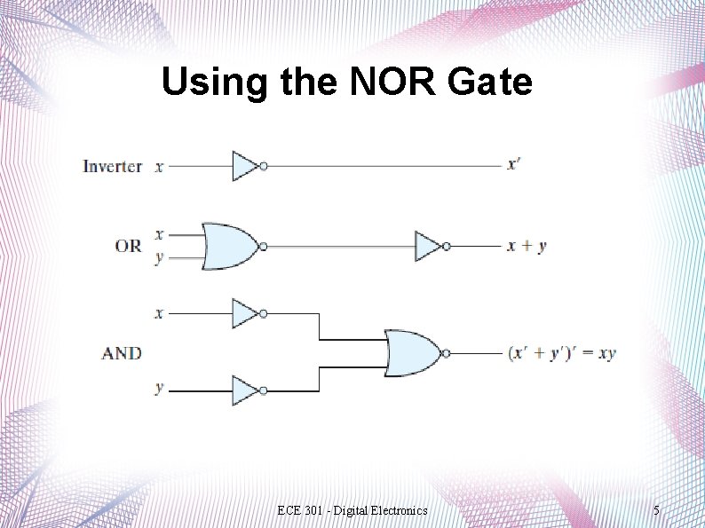
Using the NOR Gate ECE 301 - Digital Electronics 5

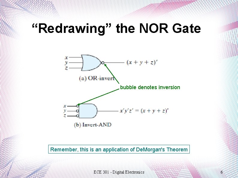
“Redrawing” the NOR Gate bubble denotes inversion Remember, this is an application of De. Morgan's Theorem ECE 301 - Digital Electronics 6

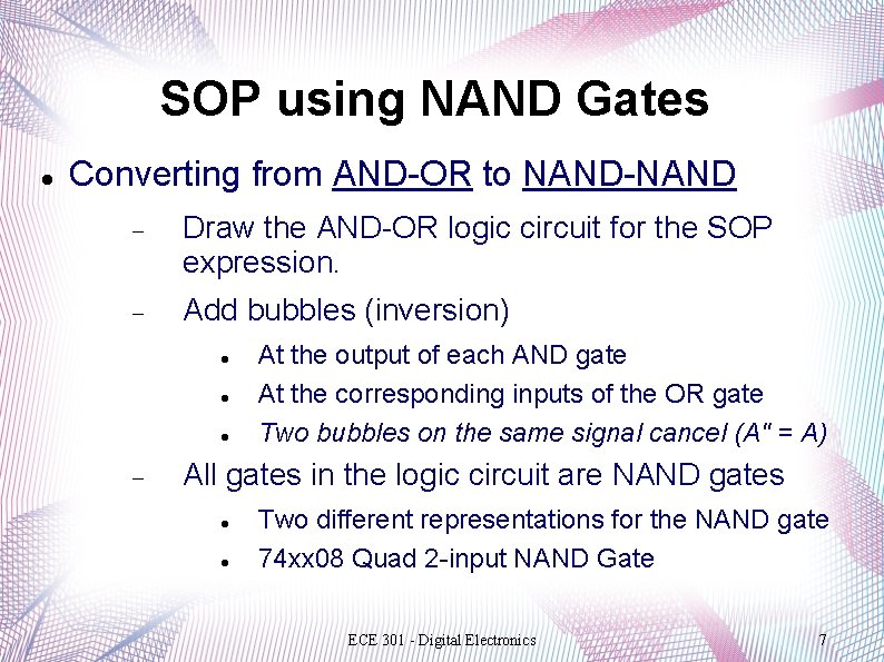
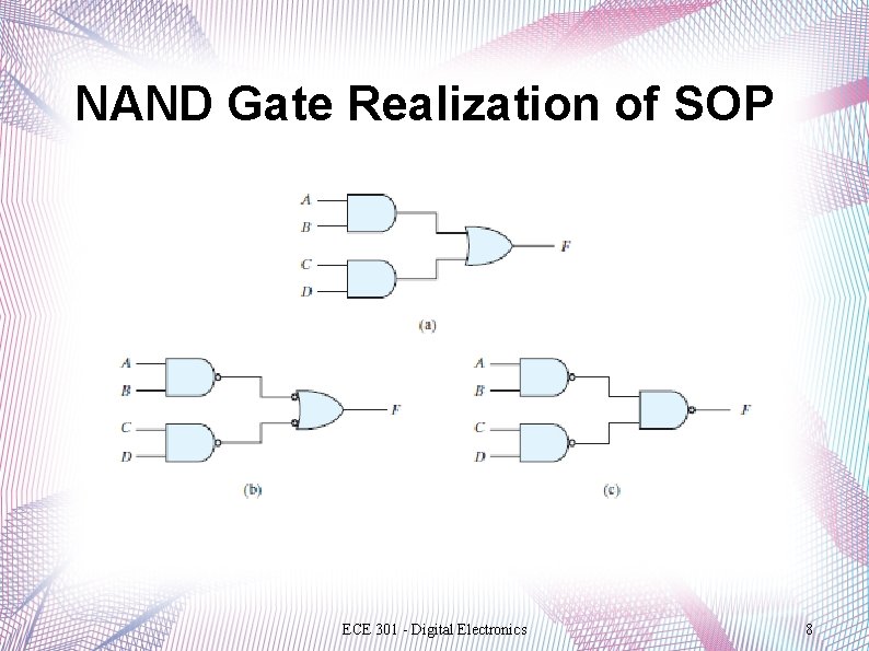
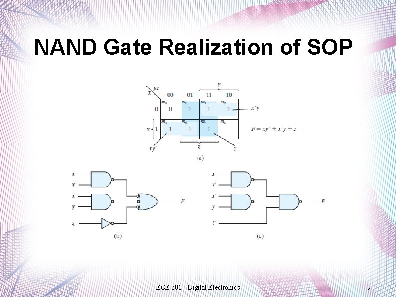
SOP using NAND Gates Converting from AND-OR to NAND-NAND Draw the AND-OR logic circuit for the SOP expression. Add bubbles (inversion) At the output of each AND gate At the corresponding inputs of the OR gate Two bubbles on the same signal cancel (A'' = A) All gates in the logic circuit are NAND gates Two different representations for the NAND gate 74 xx 08 Quad 2 -input NAND Gate ECE 301 - Digital Electronics 7

NAND Gate Realization of SOP ECE 301 - Digital Electronics 8

NAND Gate Realization of SOP ECE 301 - Digital Electronics 9

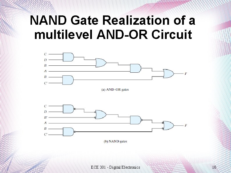
NAND Gate Realization of a multilevel AND-OR Circuit ECE 301 - Digital Electronics 10

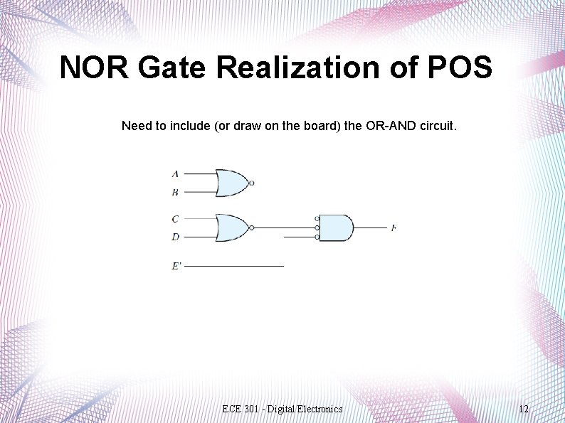
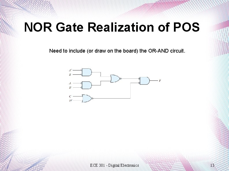
POS using NOR Gates Converting from OR-AND to NOR-NOR Draw the OR-AND logic circuit for the POS expression. Add bubbles (inversion) At the output of each OR gate At the corresponding inputs of the AND gate Two bubbles on the same signal cancel (A'' = A) All gates in the logic circuit are NOR gates Two different representations for the NOR gate 74 xx 02 Quad 2 -input NOR Gate ECE 301 - Digital Electronics 11

NOR Gate Realization of POS Need to include (or draw on the board) the OR-AND circuit. ECE 301 - Digital Electronics 12

NOR Gate Realization of POS Need to include (or draw on the board) the OR-AND circuit. ECE 301 - Digital Electronics 13

Even and Odd Logic Functions ECE 301 - Digital Electronics 14

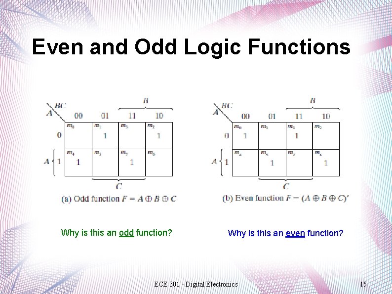
Even and Odd Logic Functions Why is this an odd function? Why is this an even function? ECE 301 - Digital Electronics 15

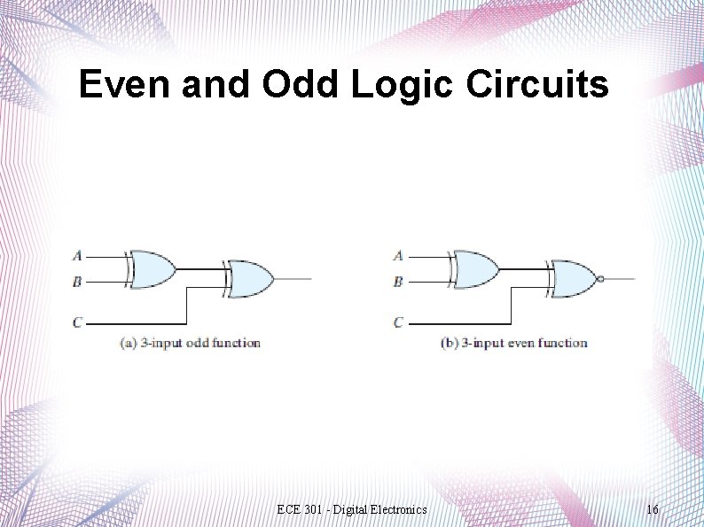
Even and Odd Logic Circuits ECE 301 - Digital Electronics 16

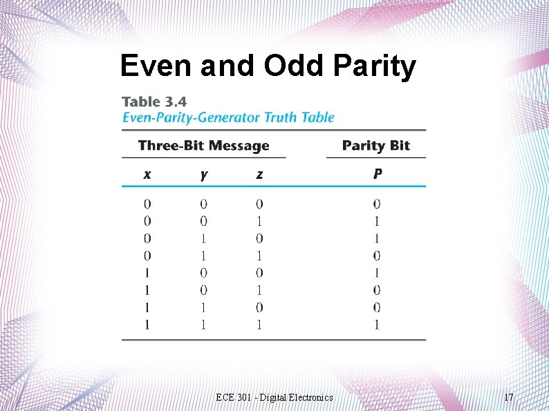
Even and Odd Parity ECE 301 - Digital Electronics 17

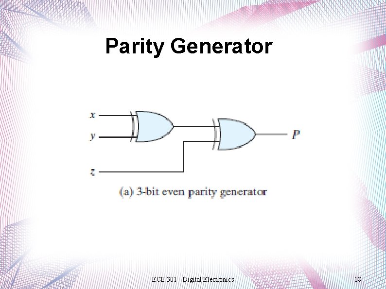
Parity Generator ECE 301 - Digital Electronics 18