MSEG 667 Nanophotonics Materials and Devices 8 Nonlinear
- Slides: 27

MSEG 667 Nanophotonics: Materials and Devices 8: Nonlinear Optics Prof. Juejun (JJ) Hu hujuejun@udel. edu “The study of non-linear physics is like the study of nonelephant biology. ” -- Stanislaw Ulam, a mathematician

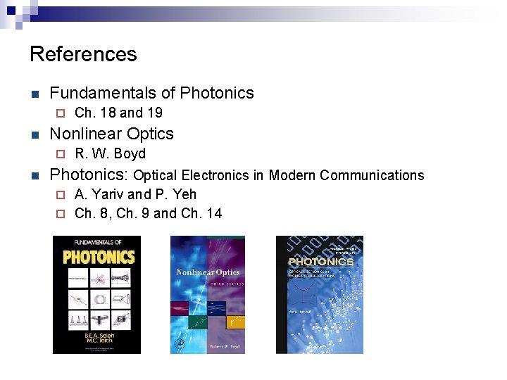
References n Fundamentals of Photonics ¨ n Nonlinear Optics ¨ n Ch. 18 and 19 R. W. Boyd Photonics: Optical Electronics in Modern Communications A. Yariv and P. Yeh ¨ Ch. 8, Ch. 9 and Ch. 14 ¨

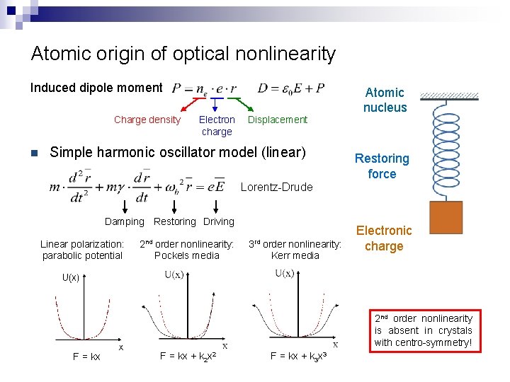
Atomic origin of optical nonlinearity Induced dipole moment Charge density n Electron charge Displacement Simple harmonic oscillator model (linear) Lorentz-Drude Damping Restoring Driving Linear polarization: parabolic potential 2 nd order nonlinearity: Pockels media 3 rd order nonlinearity: Kerr media Atomic nucleus Restoring force Electronic charge 2 nd order nonlinearity is absent in crystals with centro-symmetry! F = kx + k 2 x 2 F = kx + k 3 x 3

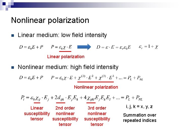
Nonlinear polarization n Linear medium: low field intensity Linear polarization n Nonlinear medium: high field intensity Nonlinear polarization Linear 2 nd order susceptibility nonlinear tensor susceptibility tensor 3 rd order nonlinear susceptibility tensor i, j, k = x, y, z Summation over repeated indices

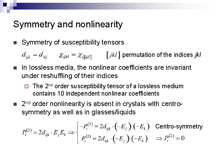
Symmetry and nonlinearity n Symmetry of susceptibility tensors permutation of the indices jkl n In lossless media, the nonlinear coefficients are invariant under reshuffling of their indices ¨ n The 2 nd order susceptibility tensor of a lossless medium contains 10 independent nonlinear coefficients 2 nd order nonlinearity is absent in crystals with centrosymmetry as well as in glasses/liquids Centro-symmetry

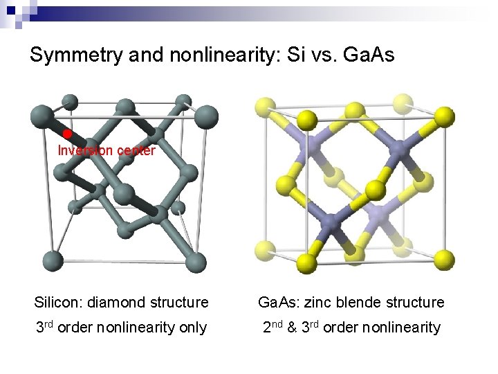
Symmetry and nonlinearity: Si vs. Ga. As Inversion center Silicon: diamond structure Ga. As: zinc blende structure 3 rd order nonlinearity only 2 nd & 3 rd order nonlinearity

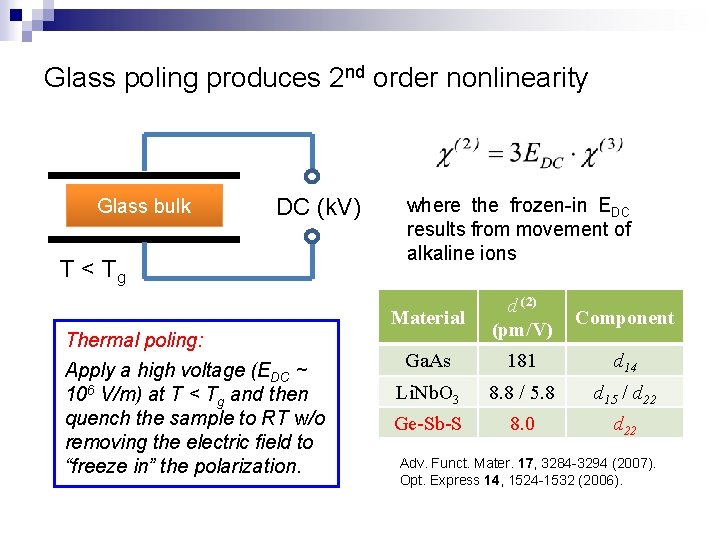
Glass poling produces 2 nd order nonlinearity Glass bulk DC (k. V) T < Tg Thermal poling: Apply a high voltage (EDC ~ 106 V/m) at T < Tg and then quench the sample to RT w/o removing the electric field to “freeze in” the polarization. where the frozen-in EDC results from movement of alkaline ions Material d (2) (pm/V) Component Ga. As 181 d 14 Li. Nb. O 3 8. 8 / 5. 8 d 15 / d 22 Ge-Sb-S 8. 0 d 22 Adv. Funct. Mater. 17, 3284 -3294 (2007). Opt. Express 14, 1524 -1532 (2006).

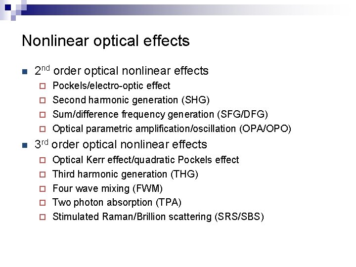
Nonlinear optical effects n 2 nd order optical nonlinear effects Pockels/electro-optic effect ¨ Second harmonic generation (SHG) ¨ Sum/difference frequency generation (SFG/DFG) ¨ Optical parametric amplification/oscillation (OPA/OPO) ¨ n 3 rd order optical nonlinear effects ¨ ¨ ¨ Optical Kerr effect/quadratic Pockels effect Third harmonic generation (THG) Four wave mixing (FWM) Two photon absorption (TPA) Stimulated Raman/Brillion scattering (SRS/SBS)

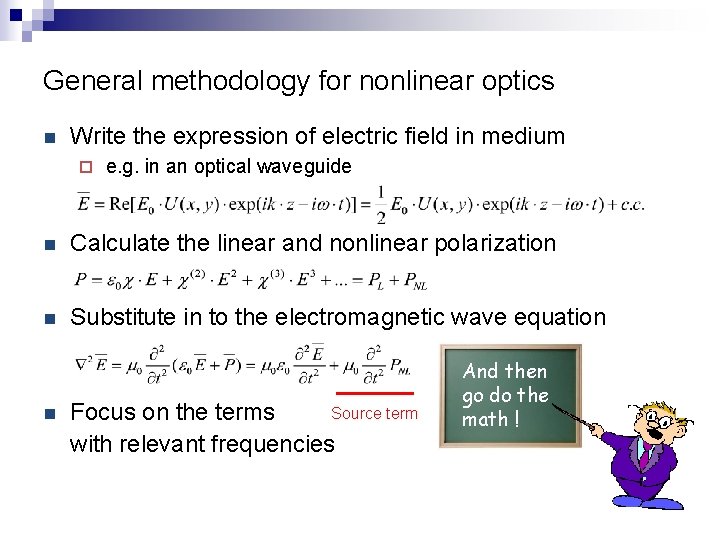
General methodology for nonlinear optics n Write the expression of electric field in medium ¨ e. g. in an optical waveguide n Calculate the linear and nonlinear polarization n Substitute in to the electromagnetic wave equation n Source term Focus on the terms with relevant frequencies And then go do the math !

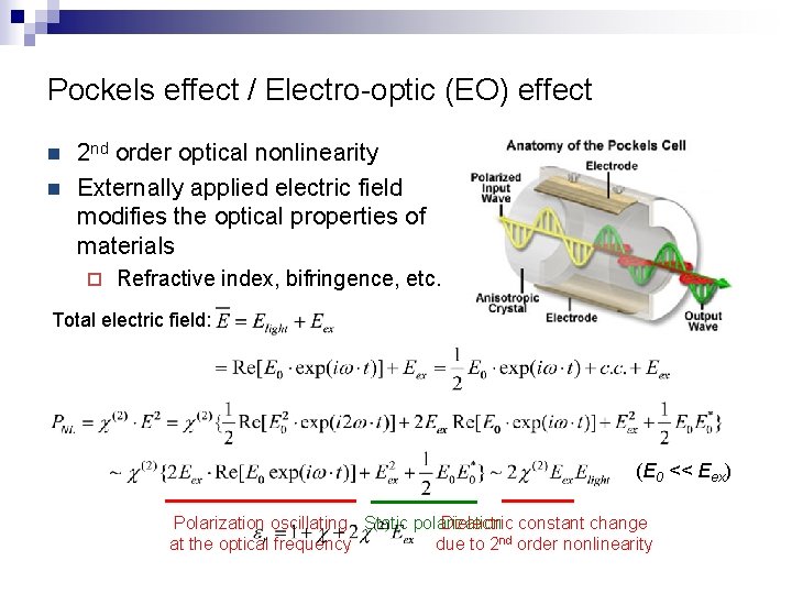
Pockels effect / Electro-optic (EO) effect n n 2 nd order optical nonlinearity Externally applied electric field modifies the optical properties of materials ¨ Refractive index, bifringence, etc. Total electric field: (E 0 << Eex) Dielectric constant change Polarization oscillating Static polarization due to 2 nd order nonlinearity at the optical frequency

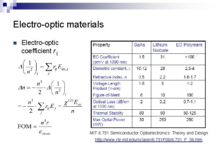
Electro-optic materials n Electro-optic coefficient rij MIT 6. 731 Semiconductor Optoelectronics: Theory and Design http: //www. rle. mit. edu/sclaser/6. 731 F 06/6. 731_F_06. htm

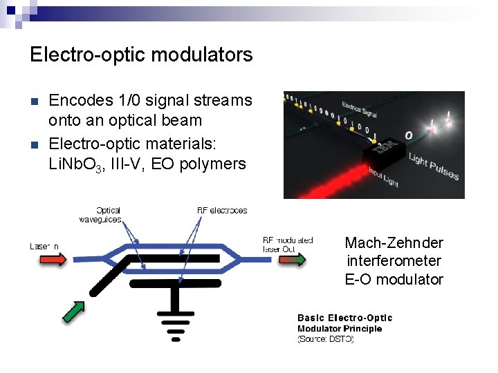
Electro-optic modulators n n Encodes 1/0 signal streams onto an optical beam Electro-optic materials: Li. Nb. O 3, III-V, EO polymers Mach-Zehnder interferometer E-O modulator

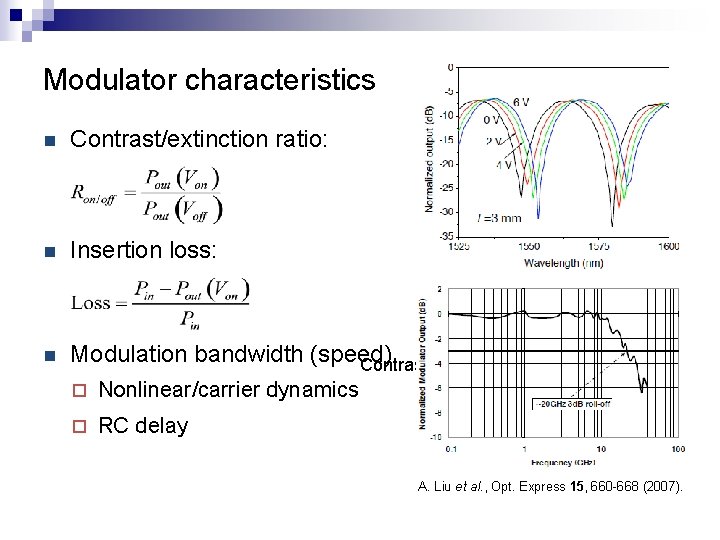
Modulator characteristics n Contrast/extinction ratio: n Insertion loss: 3 d. B bandwidth n 3 d. B Modulation bandwidth (speed) Contrast ratio (d. B) ¨ Nonlinear/carrier dynamics ¨ RC delay Modulation frequency (Hz) A. Liu et al. , Opt. Express 15, 660 -668 (2007).

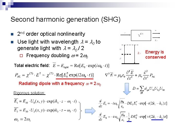
Second harmonic generation (SHG) n n 2 nd order optical nonlinearity Use light with wavelength l = l 0 to generate light with l = l 0 / 2 ¨ Frequency doubling w = 2 w 0 Total electric field: Radiating dipole with a frequency w = 2 w 0 Rigorous solution: Energy is conserved

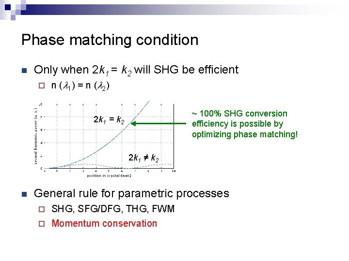
Phase matching condition n Only when 2 k 1 = k 2 will SHG be efficient ¨ n (l 1 ) = n (l 2 ) ~ 100% SHG conversion efficiency is possible by optimizing phase matching! 2 k 1 = k 2 2 k 1 ≠ k 2 n General rule for parametric processes ¨ SHG, SFG/DFG, THG, FWM ¨ Momentum conservation

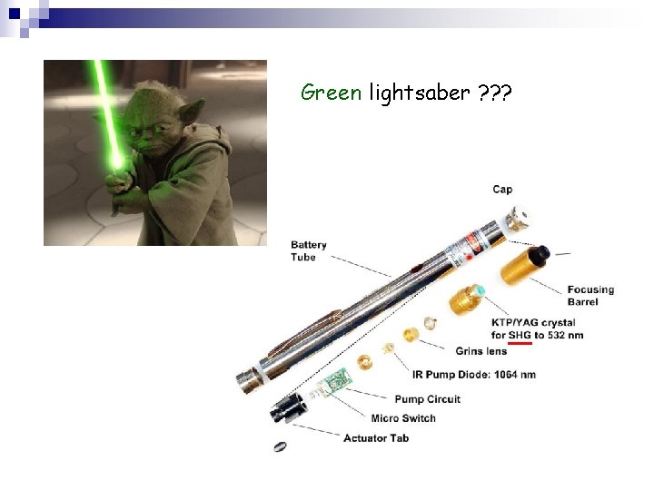
Green lightsaber ? ? ?

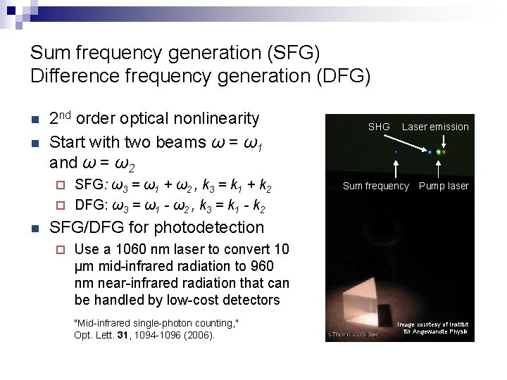
Sum frequency generation (SFG) Difference frequency generation (DFG) n n 2 nd order optical nonlinearity Start with two beams ω = ω1 and ω = ω2 SFG: ω3 = ω1 + ω2 , k 3 = k 1 + k 2 ¨ DFG: ω3 = ω1 - ω2 , k 3 = k 1 - k 2 ¨ n SHG Laser emission Sum frequency Pump laser SFG/DFG for photodetection ¨ Use a 1060 nm laser to convert 10 μm mid-infrared radiation to 960 nm near-infrared radiation that can be handled by low-cost detectors "Mid-infrared single-photon counting, " Opt. Lett. 31, 1094 -1096 (2006). Image courtesy of Institut für Angewandte Physik

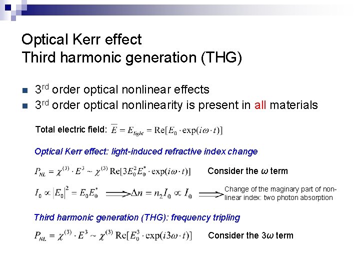
Optical Kerr effect Third harmonic generation (THG) n n 3 rd order optical nonlinear effects 3 rd order optical nonlinearity is present in all materials Total electric field: Optical Kerr effect: light-induced refractive index change Consider the ω term Change of the maginary part of nonlinear index: two photon absorption Third harmonic generation (THG): frequency tripling Consider the 3ω term

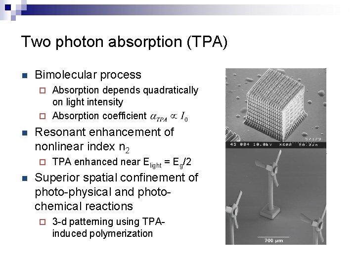
Two photon absorption (TPA) n Bimolecular process Absorption depends quadratically on light intensity ¨ Absorption coefficient ¨ n Resonant enhancement of nonlinear index n 2 ¨ n TPA enhanced near Elight = Eg/2 Superior spatial confinement of photo-physical and photochemical reactions ¨ 3 -d patterning using TPAinduced polymerization

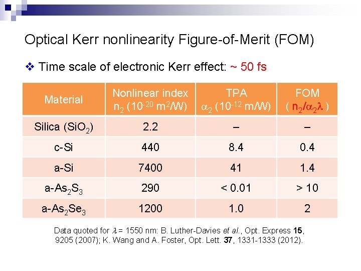
Optical Kerr nonlinearity Figure-of-Merit (FOM) v Time scale of electronic Kerr effect: ~ 50 fs Material Nonlinear index n 2 (10 -20 m 2/W) TPA a 2 (10 -12 m/W) FOM ( n 2/a 2 l ) Silica (Si. O 2) 2. 2 ‒ ‒ c-Si 440 8. 4 0. 4 a-Si 7400 41 1. 4 a-As 2 S 3 290 < 0. 01 > 10 a-As 2 Se 3 1200 1. 0 2 Data quoted for l = 1550 nm: B. Luther-Davies et al. , Opt. Express 15, 9205 (2007); K. Wang and A. Foster, Opt. Lett. 37, 1331 -1333 (2012).

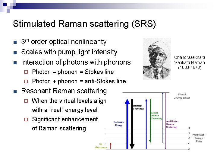
Stimulated Raman scattering (SRS) n n 3 rd order optical nonlinearity Scales with pump light intensity Interaction of photons with phonons ¨ Photon – phonon = Stokes line ¨ Photon + phonon = anti-Stokes line Resonant Raman scattering ¨ When the virtual levels align with a “real” energy level ¨ Significant enhancement of Raman scattering Chandrasekhara Venkata Raman (1888 -1970)

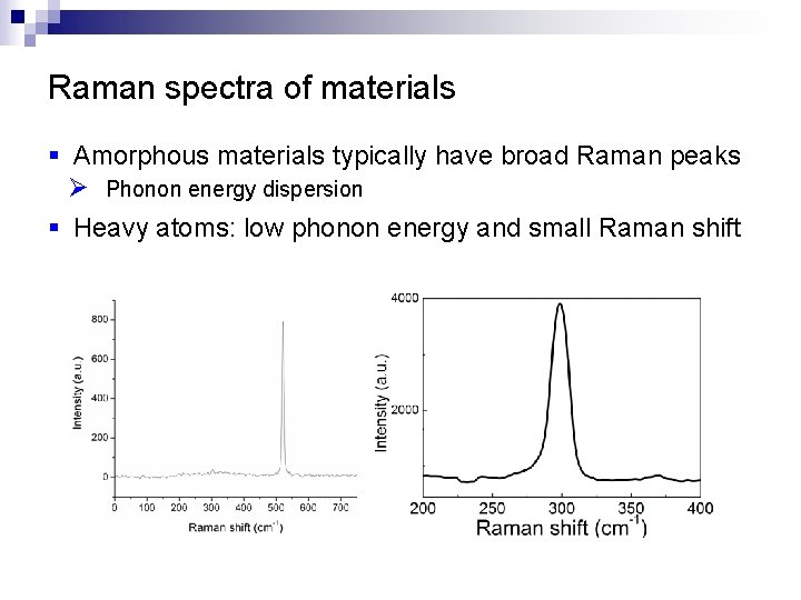
Raman spectra of materials § Amorphous materials typically have broad Raman peaks Ø Phonon energy dispersion § Heavy atoms: low phonon energy and small Raman shift

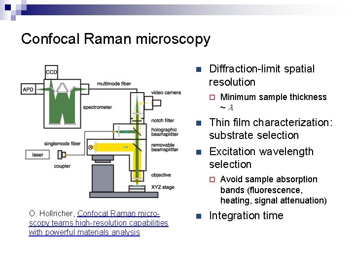
Confocal Raman microscopy n Diffraction-limit spatial resolution ¨ n n Thin film characterization: substrate selection Excitation wavelength selection ¨ O. Hollricher, Confocal Raman microscopy teams high-resolution capabilities with powerful materials analysis n Minimum sample thickness ~l Avoid sample absorption bands (fluorescence, heating, signal attenuation) Integration time

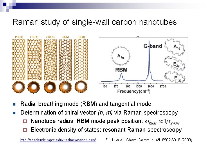
Raman study of single-wall carbon nanotubes n n Radial breathing mode (RBM) and tangential mode Determination of chiral vector (n, m) via Raman spectroscopy ¨ Nanotube radius: RBM mode peak position: ¨ Electronic density of states: resonant Raman spectroscopy http: //academic. pgcc. edu/~ssinex/nanotubes/ Z. Liu et al. , Chem. Commun. 45, 6902 -6918 (2009).

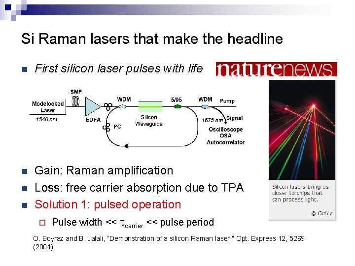
Si Raman lasers that make the headline n First silicon laser pulses with life n Gain: Raman amplification Loss: free carrier absorption due to TPA Solution 1: pulsed operation ¨ Pulse width << tcarrier << pulse period n n O. Boyraz and B. Jalali, “Demonstration of a silicon Raman laser, ” Opt. Express 12, 5269 (2004).

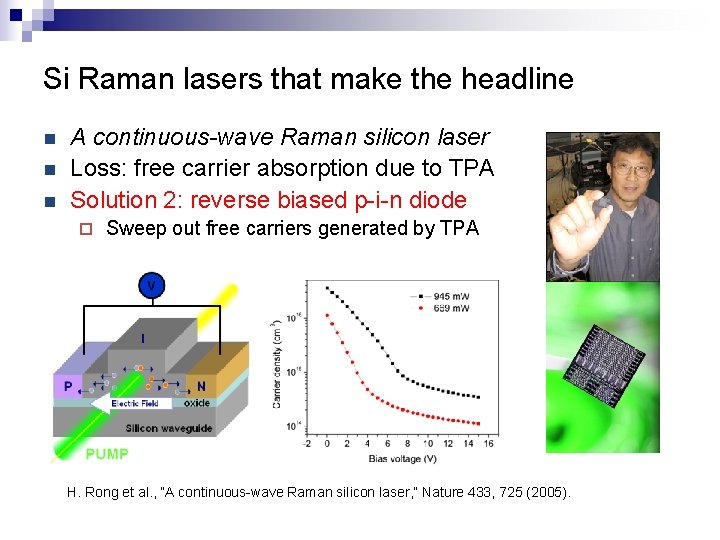
Si Raman lasers that make the headline n n n A continuous-wave Raman silicon laser Loss: free carrier absorption due to TPA Solution 2: reverse biased p-i-n diode ¨ Sweep out free carriers generated by TPA H. Rong et al. , “A continuous-wave Raman silicon laser, ” Nature 433, 725 (2005).

Si Raman lasers that make the headline n n n Loss: free carrier absorption due to TPA What is your solution to the loss issue? Solution 3: reduce free carrier life-time Introduce deep level impurities: e. g. Au/Ag ¨ Reduce waveguide size: enhanced surface recombination ¨ Increase recombination center defect density ¨ n Solution 4? ?