MS 170400714 M Tariq Shehzad CS 704 Memory

- Slides: 17

MS 170400714 M. Tariq Shehzad CS 704 Memory Hierarchies in Intel Core i 7

outline � Introduction � Basic structure of Core i 7 � Basic caching of Core i 7 � Addressing in Core i 7 � N-way set association in Core i 7 � TLB-Design in Core i 7 � Pseudo-LRU caching algorithm in Core i 7 � Conclusion

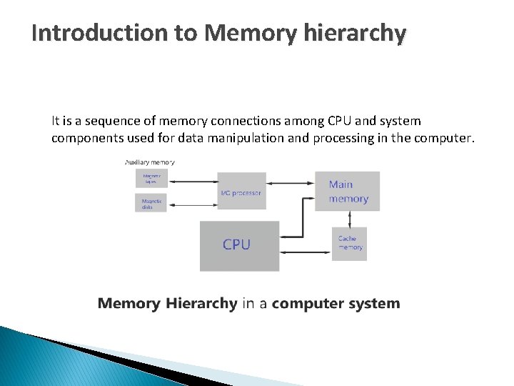
Introduction to Memory hierarchy It is a sequence of memory connections among CPU and system components used for data manipulation and processing in the computer.

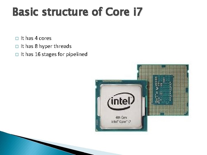
Basic structure of Core i 7 � � � It has 4 cores It has 8 hyper threads It has 16 stages for pipelined

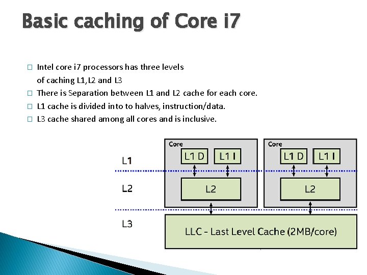
Basic caching of Core i 7 � � Intel core i 7 processors has three levels of caching L 1, L 2 and L 3 There is Separation between L 1 and L 2 cache for each core. L 1 cache is divided into to halves, instruction/data. L 3 cache shared among all cores and is inclusive.

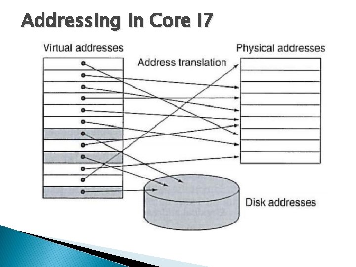
Addressing in Core i 7

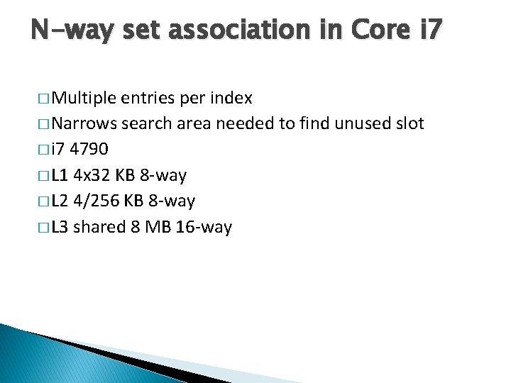
N-way set association in Core i 7 � Multiple entries per index � Narrows search area needed to find unused slot � i 7 4790 � L 1 4 x 32 KB 8 -way � L 2 4/256 KB 8 -way � L 3 shared 8 MB 16 -way

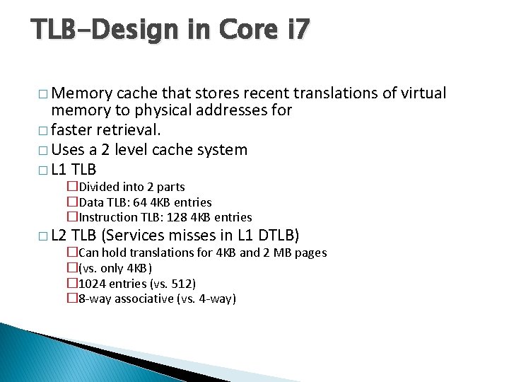
TLB-Design in Core i 7 � Memory cache that stores recent translations of virtual memory to physical addresses for � faster retrieval. � Uses a 2 level cache system � L 1 TLB �Divided into 2 parts �Data TLB: 64 4 KB entries �Instruction TLB: 128 4 KB entries � L 2 TLB (Services misses in L 1 DTLB) �Can hold translations for 4 KB and 2 MB pages �(vs. only 4 KB) � 1024 entries (vs. 512) � 8 -way associative (vs. 4 -way)

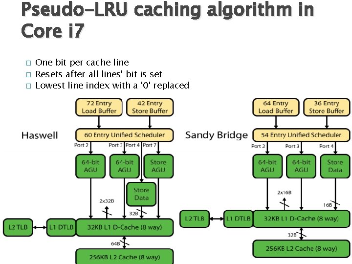
Pseudo-LRU caching algorithm in Core i 7 � � � One bit per cache line Resets after all lines' bit is set Lowest line index with a '0' replaced

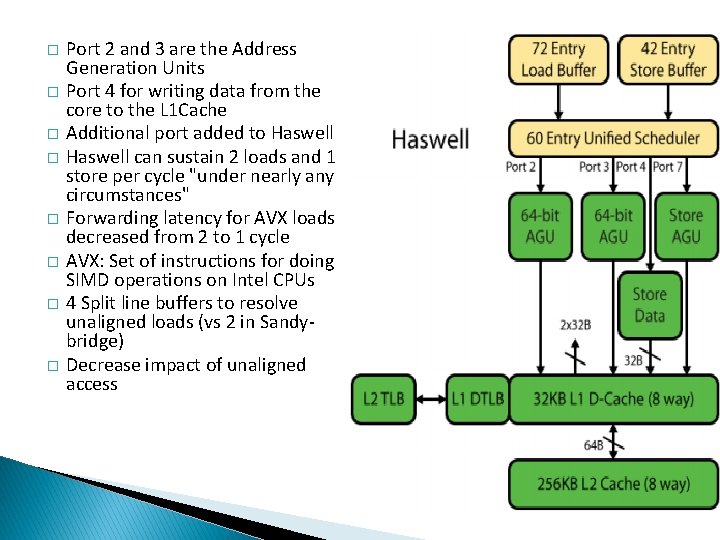
� � � � Port 2 and 3 are the Address Generation Units Port 4 for writing data from the core to the L 1 Cache Additional port added to Haswell can sustain 2 loads and 1 store per cycle "under nearly any circumstances" Forwarding latency for AVX loads decreased from 2 to 1 cycle AVX: Set of instructions for doing SIMD operations on Intel CPUs 4 Split line buffers to resolve unaligned loads (vs 2 in Sandybridge) Decrease impact of unaligned access

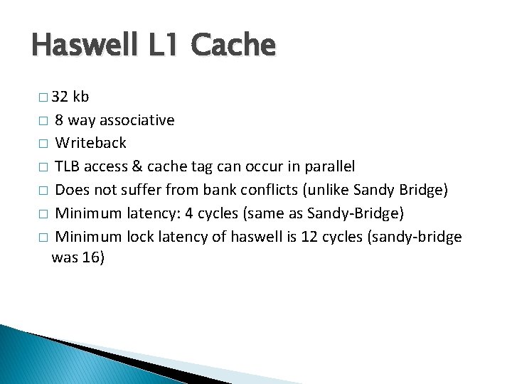
Haswell L 1 Cache � 32 kb � 8 way associative � Writeback � TLB access & cache tag can occur in parallel � Does not suffer from bank conflicts (unlike Sandy Bridge) � Minimum latency: 4 cycles (same as Sandy-Bridge) � Minimum lock latency of haswell is 12 cycles (sandy-bridge was 16)

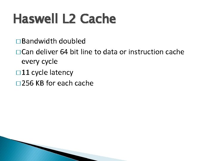
Haswell L 2 Cache � Bandwidth doubled � Can deliver 64 bit line to data or instruction cache every cycle � 11 cycle latency � 256 KB for each cache

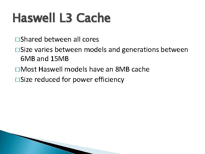
Haswell L 3 Cache � Shared between all cores � Size varies between models and generations between 6 MB and 15 MB � Most Haswell models have an 8 MB cache � Size reduced for power efficiency

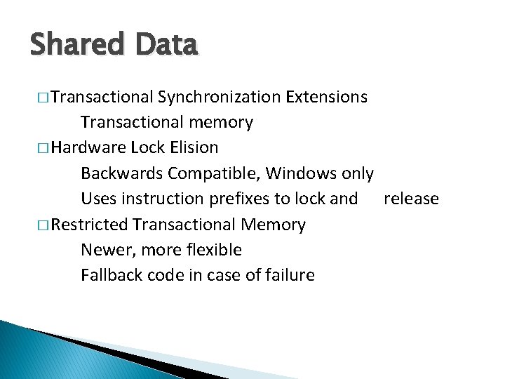
Shared Data � Transactional Synchronization Extensions Transactional memory � Hardware Lock Elision Backwards Compatible, Windows only Uses instruction prefixes to lock and release � Restricted Transactional Memory Newer, more flexible Fallback code in case of failure

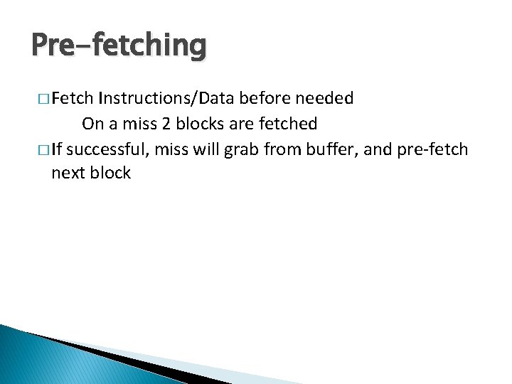
Pre-fetching � Fetch Instructions/Data before needed On a miss 2 blocks are fetched � If successful, miss will grab from buffer, and pre-fetch next block

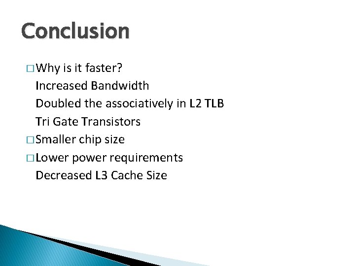
Conclusion � Why is it faster? Increased Bandwidth Doubled the associatively in L 2 TLB Tri Gate Transistors � Smaller chip size � Lower power requirements Decreased L 3 Cache Size

The End