Lecture 38 Memory 2 Last lecture Memory Architecture
- Slides: 21

Lecture #38: Memory (2) • Last lecture: – Memory Architecture – Static Ram • This lecture – Dynamic Ram – E 2 memory 12/1/2004 EE 42 fall 2004 lecture 38 1

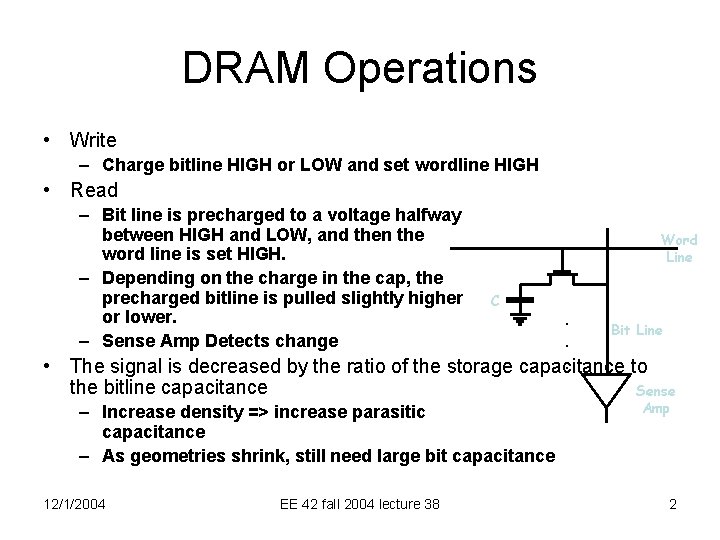
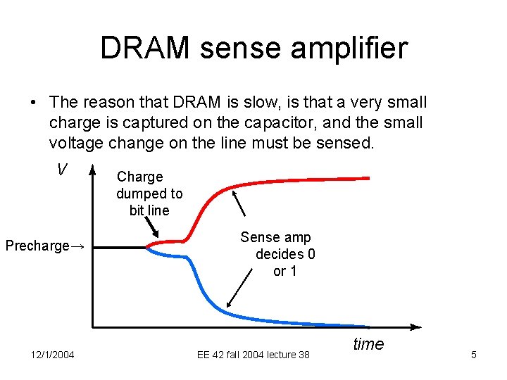
DRAM Operations • Write – Charge bitline HIGH or LOW and set wordline HIGH • Read – Bit line is precharged to a voltage halfway between HIGH and LOW, and then the word line is set HIGH. – Depending on the charge in the cap, the precharged bitline is pulled slightly higher or lower. – Sense Amp Detects change • Word Line C . Bit Line. . The signal is decreased by the ratio of the storage capacitance to the bitline capacitance – Increase density => increase parasitic capacitance – As geometries shrink, still need large bit capacitance 12/1/2004 EE 42 fall 2004 lecture 38 Sense Amp 2

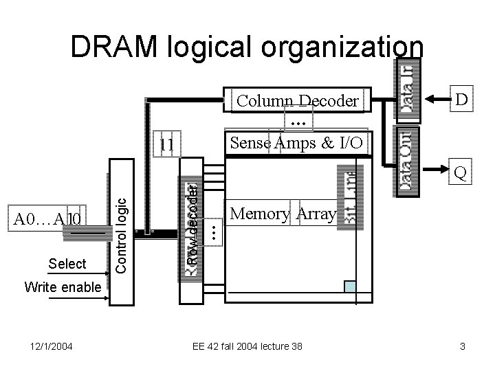
DRAM logical organization Column Decoder … Sense Amps & I/O 11 D Select Memory Array … Row decoder A 0…A 10 Control logic Q Write enable 12/1/2004 EE 42 fall 2004 lecture 38 3

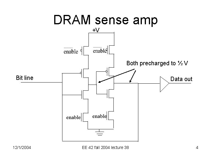
DRAM sense amp +V Both precharged to ½ V Bit line 12/1/2004 Data out EE 42 fall 2004 lecture 38 4

DRAM sense amplifier • The reason that DRAM is slow, is that a very small charge is captured on the capacitor, and the small voltage change on the line must be sensed. V Precharge→ 12/1/2004 Charge dumped to bit line Sense amp decides 0 or 1 EE 42 fall 2004 lecture 38 time 5

DRAM/SRAM tradeoffs • By it’s nature, DRAM isn’t built for speed – Response time dependent on capacitive circuit properties which get worse as density increases • DRAM process isn’t easy to integrate into CMOS process – DRAM is off chip – Connectors, wires, etc introduce slowness – IRAM efforts looking to integrating the two • Memory Architectures are designed to minimize impact of DRAM latency – Use dram for high density, store data which is used often in smaller, higher speed SRAM cache. 12/1/2004 EE 42 fall 2004 lecture 38 6

Nonvolatile memory • One disadvantage of both SRAM and DRAM is that if power is removed, the contents is lost. • One solution is to use SRAM designed to use very little current, and then to maintain power with a battery • Another solution is to use a memory type which physically alters the cell, such as EE memory 12/1/2004 EE 42 fall 2004 lecture 38 7

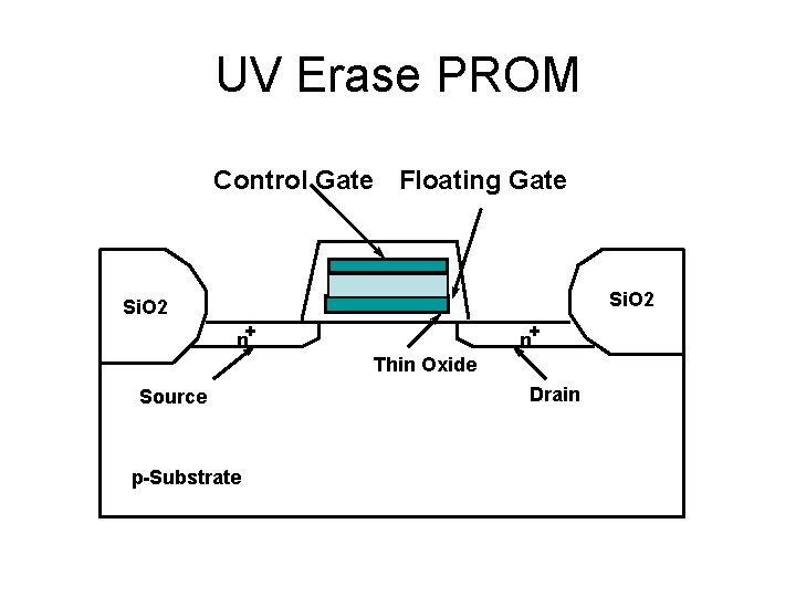
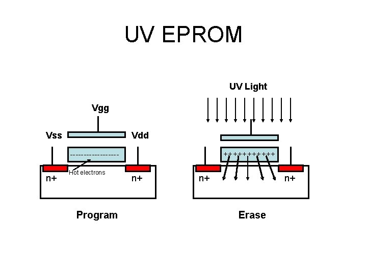
Trapped charge • Most current nonvolatile memories use a modified MOSFET with a floating gate • The floating gate can be charged or discharged by electrons moving through the oxide. • In the oldest technology, the EPROM, the floating gate is charged by hot electrons tunneling through a thin oxide, but can only be discharged by ultraviolet light exposure to the whole chip 12/1/2004 EE 42 fall 2004 lecture 38 8

UV Erase PROM Control Gate Floating Gate Si. O 2 n+ n+ Thin Oxide Source p-Substrate Drain

UV EPROM UV Light Vgg Vss Vdd --------- n+ Hot electrons Program ++++++ n+ n+ n+ Erase

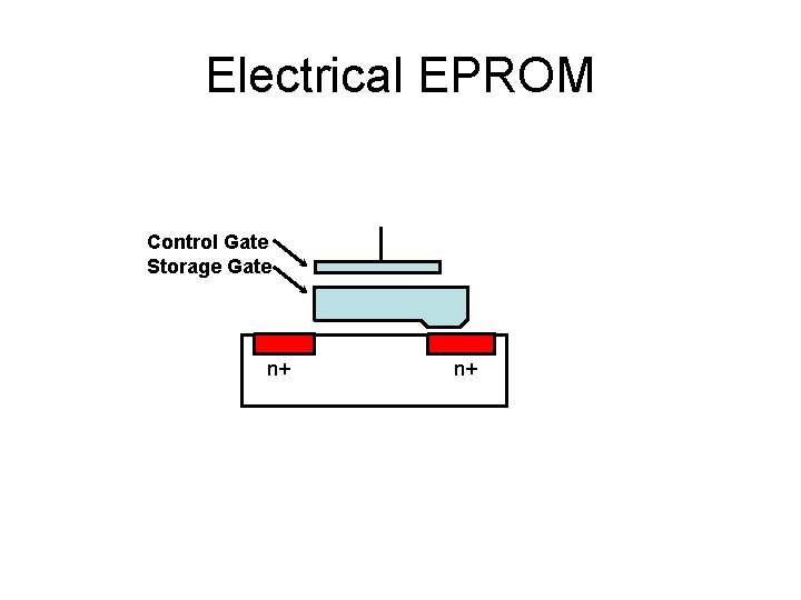
Electrical EPROM Control Gate Storage Gate n+ n+

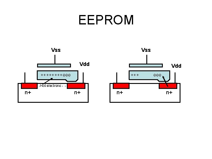
EEProm • In an EEPROM, (electrically erasable) the electrons can be tunneled back off the floating gate by applying a high voltage between the control gate and the source 12/1/2004 EE 42 fall 2004 lecture 38 12

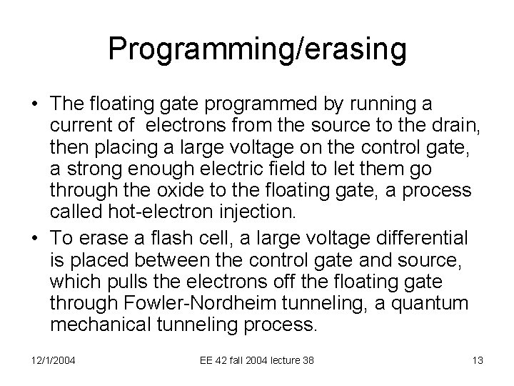
Programming/erasing • The floating gate programmed by running a current of electrons from the source to the drain, then placing a large voltage on the control gate, a strong enough electric field to let them go through the oxide to the floating gate, a process called hot-electron injection. • To erase a flash cell, a large voltage differential is placed between the control gate and source, which pulls the electrons off the floating gate through Fowler-Nordheim tunneling, a quantum mechanical tunneling process. 12/1/2004 EE 42 fall 2004 lecture 38 13

EEPROM Vss Vdd ++++eee +++ eee -Hot - - electrons ------- n+ n+

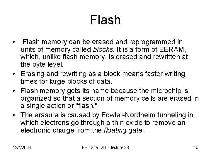
Flash • Flash memory can be erased and reprogrammed in units of memory called blocks. It is a form of EERAM, which, unlike flash memory, is erased and rewritten at the byte level. • Erasing and rewriting as a block means faster writing times for large blocks of data. • Flash memory gets its name because the microchip is organized so that a section of memory cells are erased in a single action or "flash. " • The erasure is caused by Fowler-Nordheim tunneling in which electrons go through a thin oxide to remove an electronic charge from the floating gate. 12/1/2004 EE 42 fall 2004 lecture 38 15

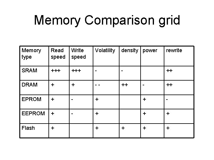
Memory Comparison grid Memory type Read speed Write speed Volatility density power rewrite SRAM +++ - - ++ DRAM + + -- ++ EPROM + - EEPROM + - Flash + - ++ + + - + + + +

Flash Memory Comparison • FLASH cells can be roughly made two or three times smaller than the EEPROM • Flash memory allows faster and more frequent programming than EPROM • Flash memory provides better data reliability than battery-backed SRAM • Flash memory fits in applications that might otherwise have used ROM (EEPROM), batterybacked RAM, or magnetic mass storage

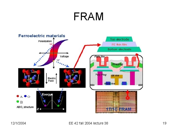
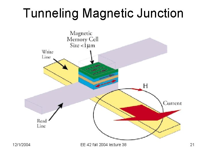
Advanced memory technologies • Ferroelectric Random Access Memory (FRAMs) • Magnetoresistive Random Access Memories (MRAMs) • Experimental Memories – Quantum-Mechanical Switch Memories – Single Electron Memory • Tunneling Magnetic Junction RAM (TMJ-RAM): – Speed of SRAM, density of DRAM, non-volatile (no refresh) – “Spintronics” electron spin effects transport – Same technology used in the read heads of high-density disk-drives: Giant magneto-resistive effect

FRAM 12/1/2004 EE 42 fall 2004 lecture 38 19

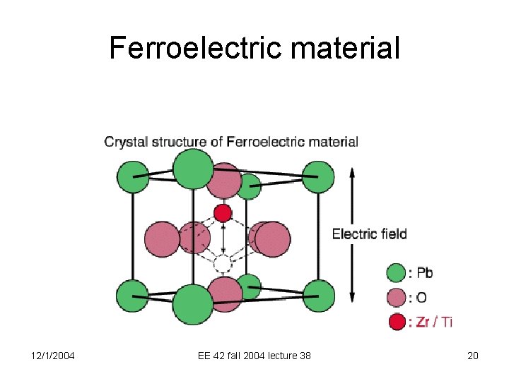
Ferroelectric material 12/1/2004 EE 42 fall 2004 lecture 38 20

Tunneling Magnetic Junction 12/1/2004 EE 42 fall 2004 lecture 38 21