International Workshop of Computational Electronics Purdue University 26

- Slides: 15

International Workshop of Computational Electronics Purdue University, 26 th of October 2004 Treatment of Point Defects in Nanowire MOSFETs Using the Nonequilibrium Green’s Function Formalism M. Bescond, J. L. Autran*, N. Cavassilas, Munteanu, and M. Lannoo Laboratoire Matériaux et Microélectronique de Provence UMR CNRS 6137 - Marseille/Toulon (France) - www. l 2 mp. fr * Also Institut Universitaire de France (IUF) D.

Outline q Introduction § MOSFETs downscaling: statistical fluctuations of doping impurity positions q 3 D Quantum simulation of point defects in nanowire transistors § Nonequilibrium Green Function formalism: Mode-Space approach § Treatment of point defects q Results: influence of the impurity location and type § Energy subbands § Transverse modes § Current characteristics q Conclusions and perspectives

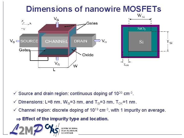
Dimensions of nanowire MOSFETs 3 ü region: Volume = L Wdoping Si TSi=10 5 3=150 ü p-type Sourcechannel and drain region: continuous of 1020 cm-3. nm 19 cm-3 1. 5 impurity on average. If doping concentration=10 ü Dimensions: L=8 nm, W =3 nm, and T =3 nm, T =1 nm. Si Si OX -3, with 1 impurity on average. ü Channel region: discreteand doping of 1019 cm Discrete distribution statistical location. Effect of the impurity type and location.

Nonequilibrium Green’s function formalism Point Defect Treatment

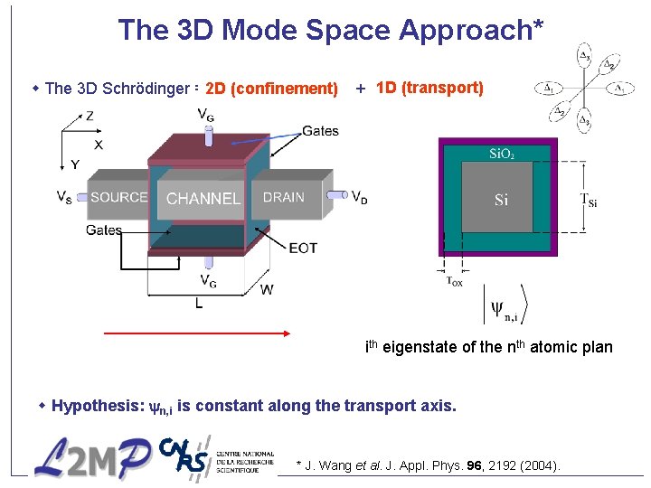
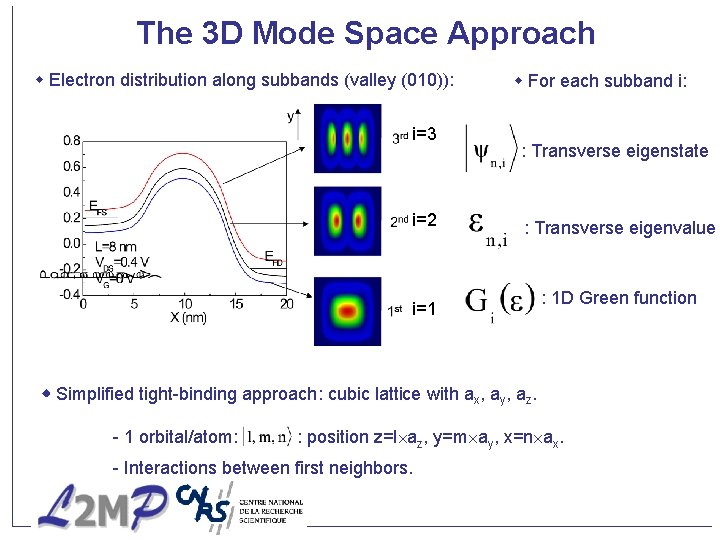
The 3 D Mode Space Approach* The 3 D Schrödinger = 2 D 2 D (confinement) 1 D( (transport) + 1 D transport) ith eigenstate of the nth atomic plan Hypothesis: n, i is constant along the transport axis. * J. Wang et al. J. Appl. Phys. 96, 2192 (2004).

The 3 D Mode Space Approach Electron distribution along subbands (valley (010)): i=3 i=2 For each subband i: : Transverse eigenstate : Transverse eigenvalue i=1 : 1 D Green function Simplified tight-binding approach: cubic lattice with ax, ay, az. - 1 orbital/atom: : position z=l az, y=m ay, x=n ax. - Interactions between first neighbors.

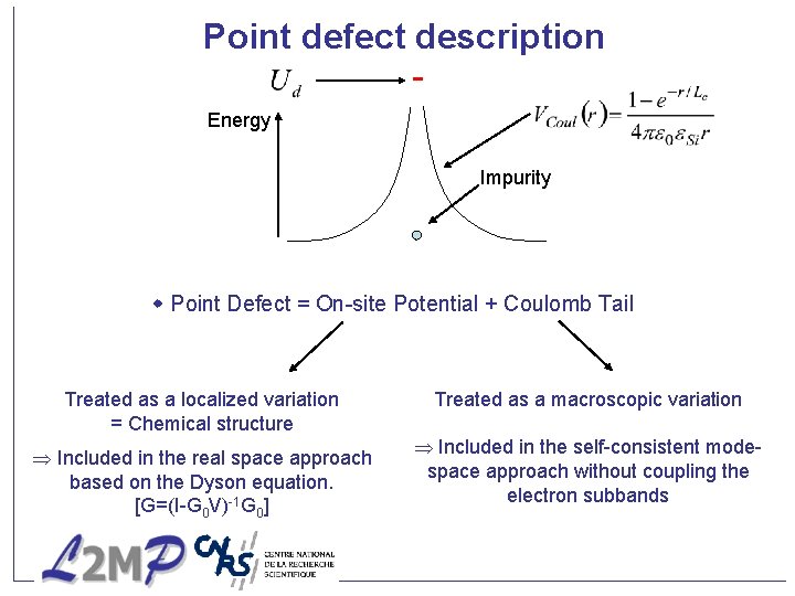
Point defect description Energy Impurity Point Defect = On-site Potential + Coulomb Tail Treated as a localized variation = Chemical structure Included in the real space approach based on the Dyson equation. [G=(I-G 0 V)-1 G 0] Treated as a macroscopic variation Included in the self-consistent modespace approach without coupling the electron subbands

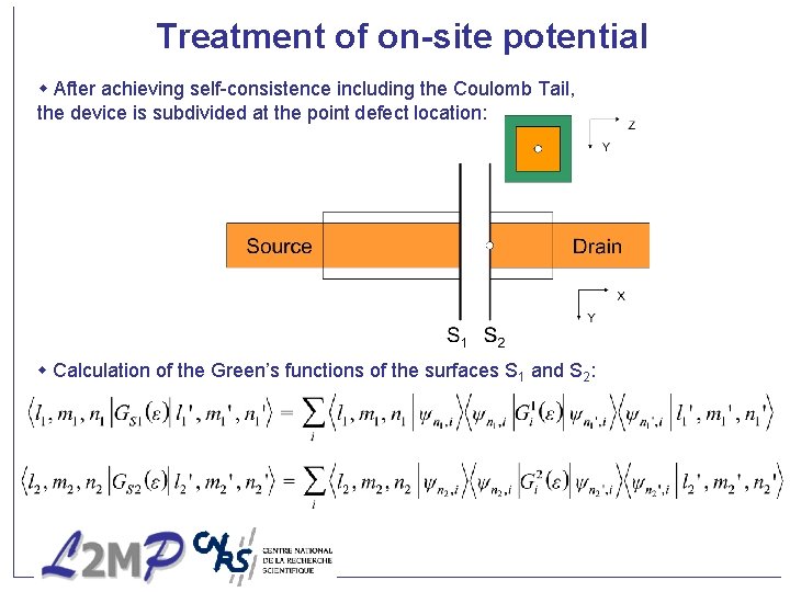
Treatment of on-site potential After achieving self-consistence including the Coulomb Tail, the device is subdivided at the point defect location: Calculation of the Green’s functions of the surfaces S 1 and S 2:

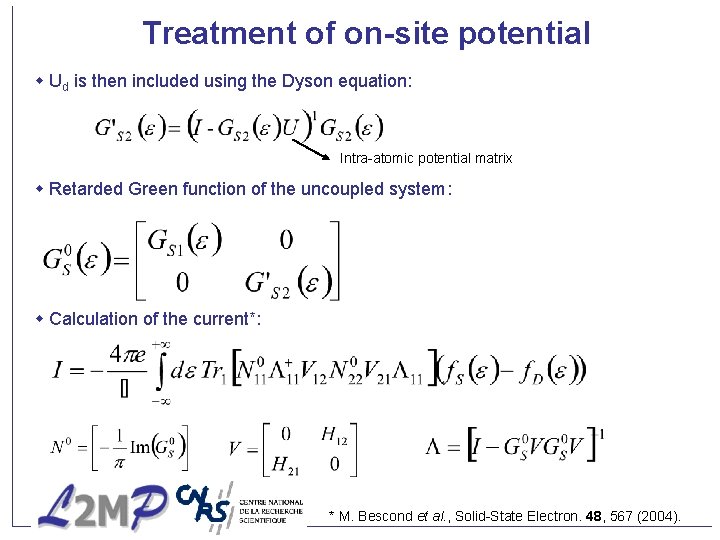
Treatment of on-site potential Ud is then included using the Dyson equation: Intra-atomic potential matrix Retarded Green function of the uncoupled system: Calculation of the current*: * M. Bescond et al. , Solid-State Electron. 48, 567 (2004).

Results Influence of point defect

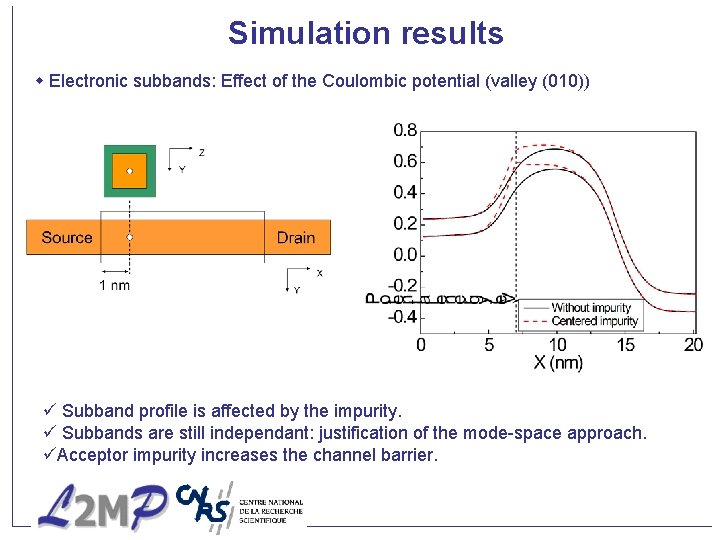
Simulation results Electronic subbands: Effect of the Coulombic potential (valley (010)) ü Subband profile is affected by the impurity. ü Subbands are still independant: justification of the mode-space approach. üAcceptor impurity increases the channel barrier.

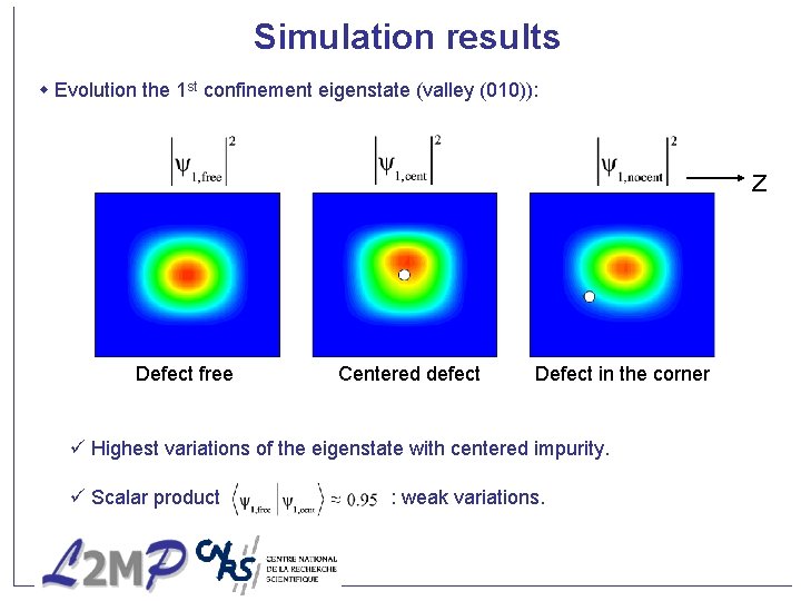
Simulation results Evolution the 1 st confinement eigenstate (valley (010)): z Defect free Centered defect Defect in the corner ü Highest variations of the eigenstate with centered impurity. ü Scalar product : weak variations.

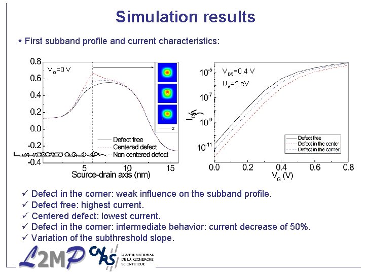
Simulation results First subband profile and current characteristics: VG=0 V VDS=0. 4 V Ud=2 e. V ü Defect in the corner: weak influence on the subband profile. ü Defect free: highest current. ü Centered defect: lowest current. ü Defect in the corner: intermediate behavior: current decrease of 50%. ü Variation of the subthreshold slope.

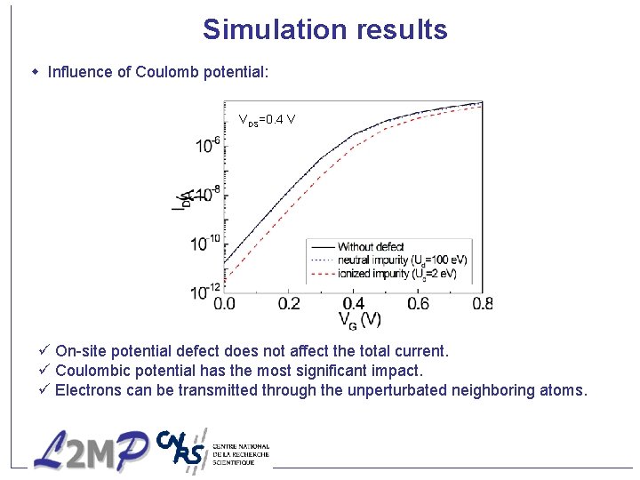
Simulation results Influence of Coulomb potential: VDS=0. 4 V ü On-site potential defect does not affect the total current. ü Coulombic potential has the most significant impact. ü Electrons can be transmitted through the unperturbated neighboring atoms.

Conclusion Modeling of electron-ion interaction based on the NEGF formalism. Study of the effect the acceptor impurity in terms of physical properties. Centered impurity involves a significant degradation of the current. Not only a shift of the current but rather a subthreshold slope variation. The Coulomb potential has a prevalent rule compared to the on-site potential of the impurity. Treatment of donor impurities in source and drain.