https indico cern chevent640107 Depleted Monolithic Active Pixel


- Slides: 18

https: //indico. cern. ch/event/640107/ Depleted Monolithic Active Pixel Sensors for ATLAS Upgrade Dima Maneuski et. al.

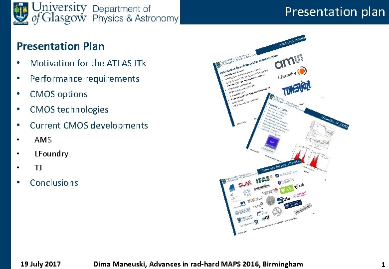
Presentation plan Presentation Plan • Motivation for the ATLAS ITk • Performance requirements • CMOS options • CMOS technologies • Current CMOS developments • AMS • LFoundry • TJ • Conclusions 19 July 2017 Dima Maneuski, Advances in rad-hard MAPS 2016, Birmingham 1

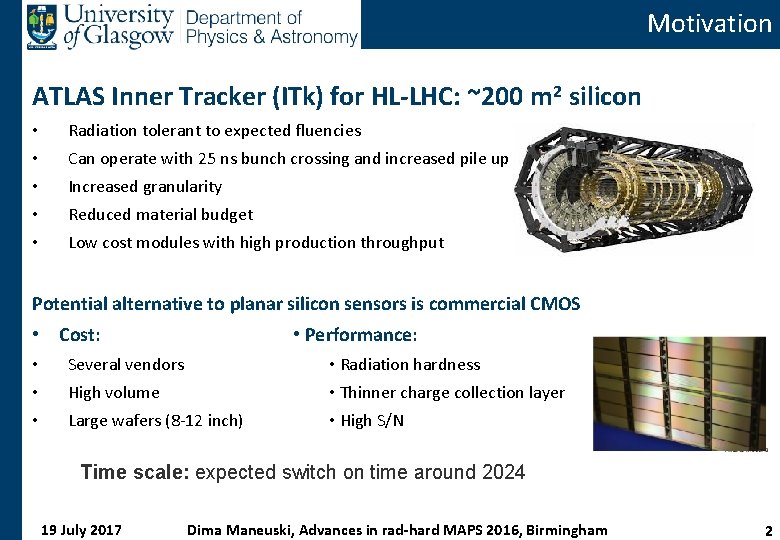
Motivation ATLAS Inner Tracker (ITk) for HL-LHC: ~200 m 2 silicon • Radiation tolerant to expected fluencies • Can operate with 25 ns bunch crossing and increased pile up • Increased granularity • Reduced material budget • Low cost modules with high production throughput Potential alternative to planar silicon sensors is commercial CMOS • Performance: • Cost: • Several vendors • Radiation hardness • High volume • Thinner charge collection layer • Large wafers (8 -12 inch) • High S/N Time scale: expected switch on time around 2024 19 July 2017 Dima Maneuski, Advances in rad-hard MAPS 2016, Birmingham 2

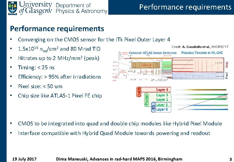
Performance requirements • Converging on the CMOS sensor for the ITk Pixel Outer Layer 4 • 1. 5 x 10¹⁵ neq/cm 2 and 80 Mrad TID Credit: A. Gaudiello et al. , IWORID’ 17 • Hitrates up to 2 MHz/mm 2 (peak) • Timing: < 25 ns • Efficiency: > 95% after irradiations • Pixel size: < 50 um • Chip size like ATLAS-1 Pixel FE chip • CMOS to be integrated into quad and double chip modules like Hybrid Pixel Module • Interface compatible with Hybrid Quad Module towards powering and readout 19 July 2017 Dima Maneuski, Advances in rad-hard MAPS 2016, Birmingham 3

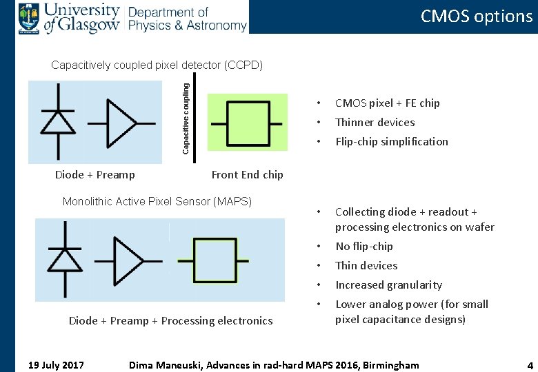
CMOS options Capacitive coupling Capacitively coupled pixel detector (CCPD) Diode + Preamp CMOS pixel + FE chip • Thinner devices • Flip-chip simplification • Collecting diode + readout + processing electronics on wafer • No flip-chip • Thin devices • Increased granularity • Lower analog power (for small pixel capacitance designs) Front End chip Monolithic Active Pixel Sensor (MAPS) Diode + Preamp + Processing electronics 19 July 2017 • Dima Maneuski, Advances in rad-hard MAPS 2016, Birmingham 4

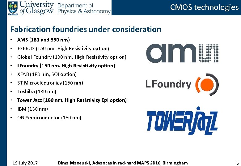
CMOS technologies Fabrication foundries under consideration • AMS (180 and 350 nm) • ESPROS (150 nm, High Resistivity option) • Global Foundry (130 nm, High Resistivity option) • LFoundry (150 nm, High Resistivity option) • XFAB (180 nm, SOI option) • ST Microelectronics (160 nm) • Toshiba (130 nm) • Tower Jazz (180 nm, High Resistivity Epi option) • IBM (130 nm) • ON Semiconductor (180 nm) 19 July 2017 Dima Maneuski, Advances in rad-hard MAPS 2016, Birmingham 5

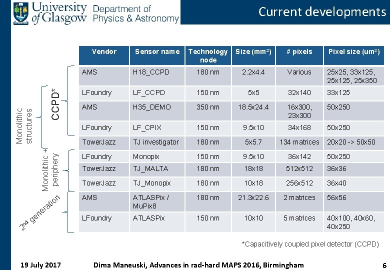
Current developments CCPD* Monolithic + periphery Monolithic structures Vendor nd 2 n io t ra e n ge Sensor name Technology node Size (mm 2) # pixels Pixel size (um 2) AMS H 18_CCPD 180 nm 2. 2 x 4. 4 Various 25 x 25, 33 x 125, 25 x 350 LFoundry LF_CCPD 150 nm 5 x 5 32 x 140 33 x 125 AMS H 35_DEMO 350 nm 18. 5 x 24. 4 16 x 300, 23 x 300 50 x 250 LFoundry LF_CPIX 150 nm 9. 5 x 10 34 x 168 50 x 250 Tower. Jazz TJ investigator 180 nm 5 x 5. 7 134 matrices LFoundry Monopix 150 nm 9. 5 x 10 36 x 142 50 x 250 Tower. Jazz TJ_MALTA 180 nm 18 x 18 512 x 512 36 x 36 Tower. Jazz TJ_Monopix 180 nm 10 x 18 256 x 512 36 x 40 AMS ATLASPix / Mu. Pix 8 180 nm 21. 3 x 22. 6 2 matrices 56 x 56 LFoundry ATLASPix 150 nm 10 x 10 5 matrices 40 x 100, 40 x 60, 40 x 250 20 x 20 -> 50 x 50 *Capacitively coupled pixel detector (CCPD) 19 July 2017 Dima Maneuski, Advances in rad-hard MAPS 2016, Birmingham 6

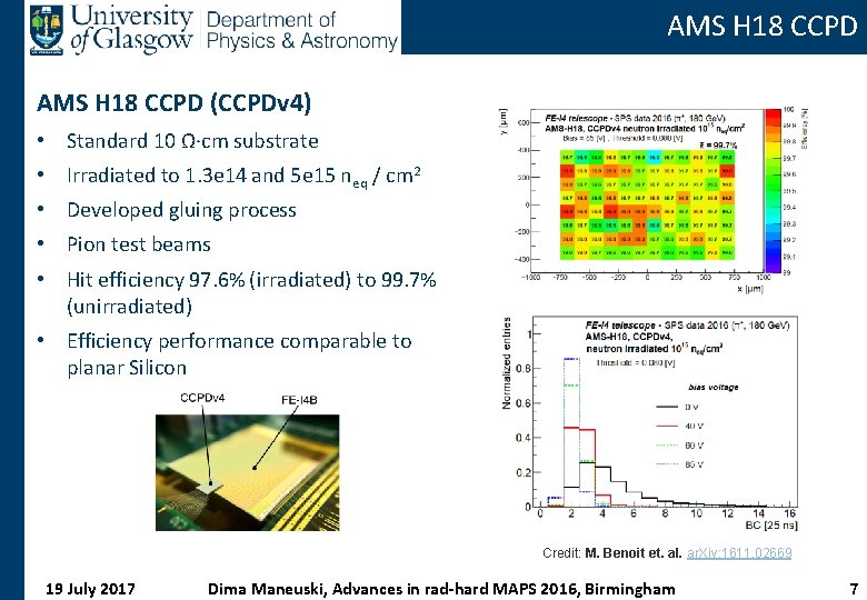
AMS H 18 CCPD (CCPDv 4) • Standard 10 Ω·cm substrate • Irradiated to 1. 3 e 14 and 5 e 15 neq / cm 2 • Developed gluing process • Pion test beams • Hit efficiency 97. 6% (irradiated) to 99. 7% (unirradiated) • Efficiency performance comparable to planar Silicon Credit: M. Benoit et. al. ar. Xiv: 1611. 02669 19 July 2017 Dima Maneuski, Advances in rad-hard MAPS 2016, Birmingham 7

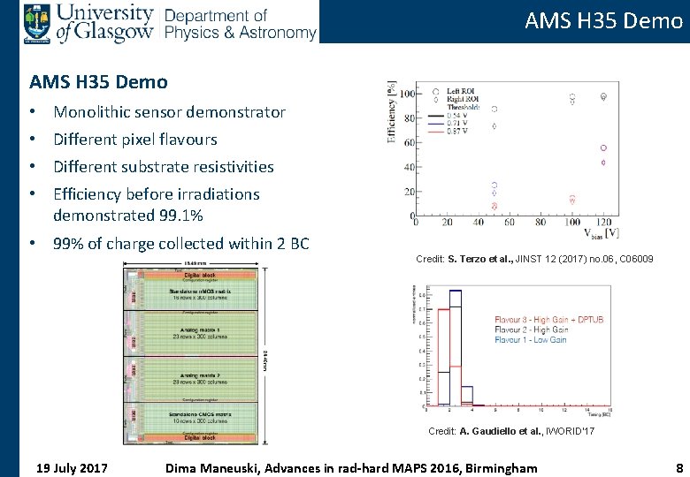
AMS H 35 Demo • Monolithic sensor demonstrator • Different pixel flavours • Different substrate resistivities • Efficiency before irradiations demonstrated 99. 1% • 99% of charge collected within 2 BC Credit: S. Terzo et al. , JINST 12 (2017) no. 06, C 06009 Credit: A. Gaudiello et al. , IWORID’ 17 19 July 2017 Dima Maneuski, Advances in rad-hard MAPS 2016, Birmingham 8

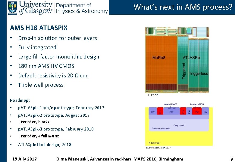
What’s next in AMS process? AMS H 18 ATLASPIX • Drop-in solution for outer layers • Fully integrated • Large fill factor monolithic design • 180 nm AMS HV CMOS • Default resistivity is 20 Ω cm • Triple well process Roadmap: • p. ATLASpix-1 a/b/c prototype, February 2017 • p. ATLASpix-2 prototype, August 2017 • • Periphery blocks p. ATLASpix-3 prototype, February 2018 Periphery + full matrix ATLASpix final design, 2018 19 July 2017 Dima Maneuski, Advances in rad-hard MAPS 2016, Birmingham 9

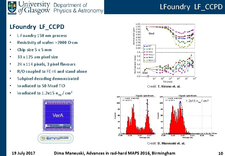
LFoundry LF_CCPD • L-Foundry 150 nm process • Resistivity of wafer: >2000 Ω·cm • Chip size 5 x 5 mm • 33 x 125 um pixel size • 24 x 114 pixels, 3 pixel flavours • R/O coupled to FE-I 4 and stand alone • Subpixel decoding demonstrated • Irradiated to 50 Mrad TID • Irradiated to 1. 2 e 15 neq / cm 2 Credit: T. Hirono et. al. 1. 2 e 15 neq / cm 2 Credit: D. Maneuski et. al. 19 July 2017 Dima Maneuski, Advances in rad-hard MAPS 2016, Birmingham 10

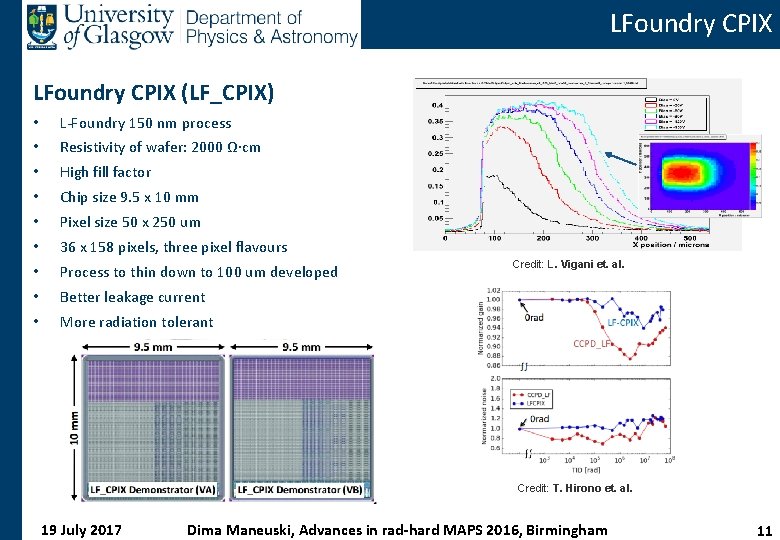
LFoundry CPIX (LF_CPIX) • L-Foundry 150 nm process • Resistivity of wafer: 2000 Ω·cm • High fill factor • Chip size 9. 5 x 10 mm • Pixel size 50 x 250 um • 36 x 158 pixels, three pixel flavours • Process to thin down to 100 um developed • Better leakage current • More radiation tolerant Credit: L. Vigani et. al. Credit: T. Hirono et. al. 19 July 2017 Dima Maneuski, Advances in rad-hard MAPS 2016, Birmingham 11

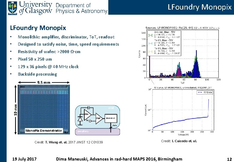
LFoundry Monopix • Monolithic: amplifier, discriminator, To. T, readout • Designed to satisfy noise, time, speed requirements • Resistivity of wafer: >2000 Ω·cm • Pixel 50 x 250 um • 129 x 36 pixels @ 40 MHz clock • Backside processing Credit: T. Wang et. al. 2017 JINST 12 C 01039 19 July 2017 Credit: I. Caicedo et. al. Dima Maneuski, Advances in rad-hard MAPS 2016, Birmingham 12

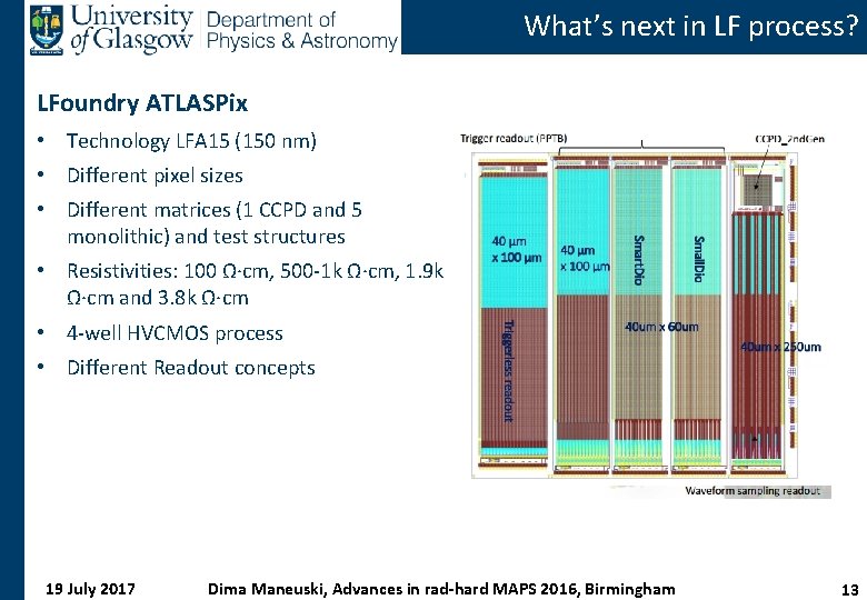
What’s next in LF process? LFoundry ATLASPix • Technology LFA 15 (150 nm) • Different pixel sizes • Different matrices (1 CCPD and 5 monolithic) and test structures • Resistivities: 100 Ω·cm, 500 -1 k Ω·cm, 1. 9 k Ω·cm and 3. 8 k Ω·cm • 4 -well HVCMOS process • Different Readout concepts 19 July 2017 Dima Maneuski, Advances in rad-hard MAPS 2016, Birmingham 13

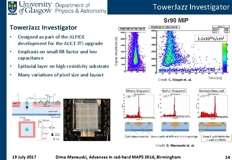
Tower. Jazz Investigator Sr 90 MIP • Designed as part of the ALPIDE development for the ALICE ITS upgrade • Emphasis on small fill-factor and low capacitance • Epitaxial layer on high resistivity substrate • Many variations of pixel size and layout Signal Amplitude [e] Tower. Jazz Investigator Credit: C. Riegel et. al. Time [ns] Credit: D. Maneuski et. al. 19 July 2017 Dima Maneuski, Advances in rad-hard MAPS 2016, Birmingham 14

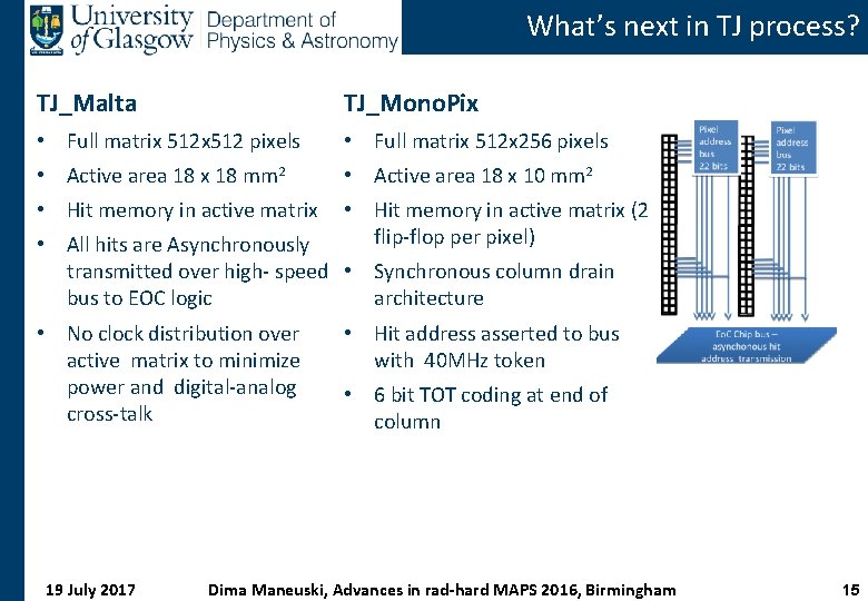
What’s next in TJ process? TJ_Malta TJ_Mono. Pix • Full matrix 512 pixels • Full matrix 512 x 256 pixels • Active area 18 x 18 mm 2 • Active area 18 x 10 mm 2 • Hit memory in active matrix (2 flip-flop per pixel) • All hits are Asynchronously transmitted over high- speed • Synchronous column drain bus to EOC logic architecture • No clock distribution over active matrix to minimize power and digital-analog cross-talk 19 July 2017 • Hit address asserted to bus with 40 MHz token • 6 bit TOT coding at end of column Dima Maneuski, Advances in rad-hard MAPS 2016, Birmingham 15

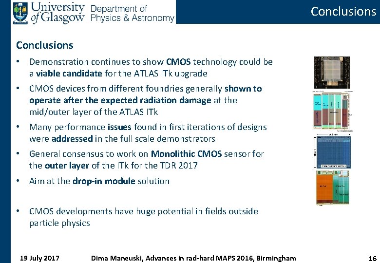
Conclusions • Demonstration continues to show CMOS technology could be a viable candidate for the ATLAS ITk upgrade • CMOS devices from different foundries generally shown to operate after the expected radiation damage at the mid/outer layer of the ATLAS ITk • Many performance issues found in first iterations of designs were addressed in the full scale demonstrators • General consensus to work on Monolithic CMOS sensor for the outer layer of the ITk for the TDR 2017 • Aim at the drop-in module solution • CMOS developments have huge potential in fields outside particle physics 19 July 2017 Dima Maneuski, Advances in rad-hard MAPS 2016, Birmingham 16

Thank you for your attention Any 19 July 2017 Dima Maneuski, Advances in rad-hard MAPS 2016, Birmingham s? n o i t ques 17