Monolithic and Vertically Integrated Pixel Detectors CERN 25
- Slides: 16

Monolithic and Vertically Integrated Pixel Detectors, CERN, 25 th November 2008 CMOS Monolithic Active Pixel Sensors R. Turchetta CMOS Sensor Design Group Rutherford Appleton Laboratory, Oxfordshire, UK

2 Outline Ø CMOS Image Sensors @ RAL Ø The INMAPS process and its silicon proof Ø Conclusions

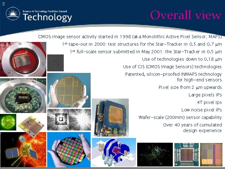
3 Overall view CMOS image sensor activity started in 1998 (aka Monolithic Active Pixel Sensor; MAPS) 1 st tape-out in 2000: test structures for the Star-Tracker in 0. 5 and 0. 7 mm 1 st full-scale sensor submitted in May 2001: the Star-Tracker in 0. 5 mm Use of technologies down to 0. 18 mm Use of CIS (CMOS Image Sensors) technologies Patented, silicon-proofed INMAPS technology for high-end sensors Pixel size from 2 mm upwards Large pixels IPs 4 T pixel Ips Low noise pixel IPs Wafer-scale (200 mm) sensor capability Over 40 years of cumulated design experience

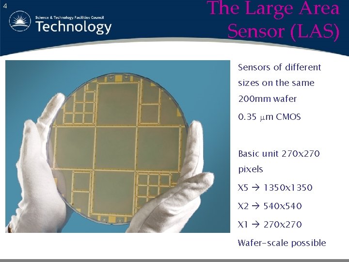
4 The Large Area Sensor (LAS) Sensors of different sizes on the same 200 mm wafer 0. 35 mm CMOS Basic unit 270 x 270 pixels X 5 1350 x 1350 X 2 540 x 540 X 1 270 x 270 Wafer-scale possible

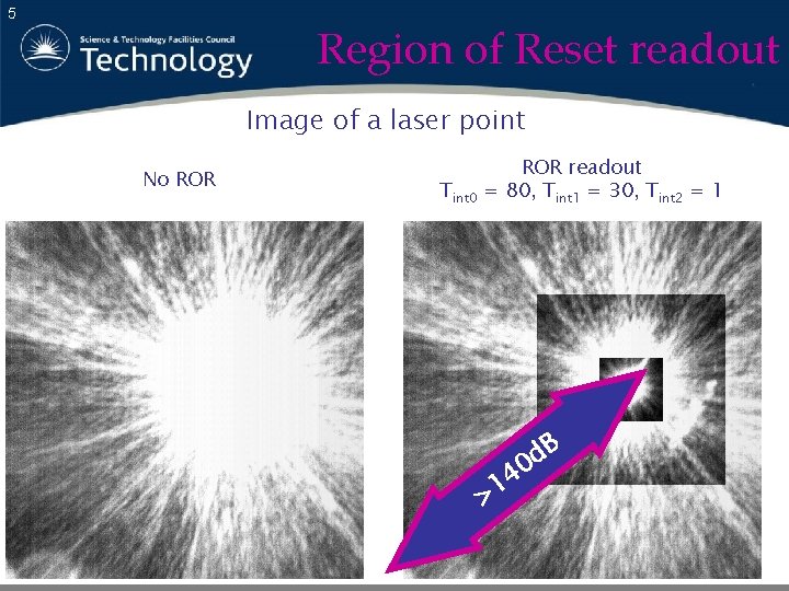
5 Region of Reset readout Image of a laser point No ROR Tint 0 ROR readout = 80, Tint 1 = 30, Tint 2 = 1 4 1 > B d 0

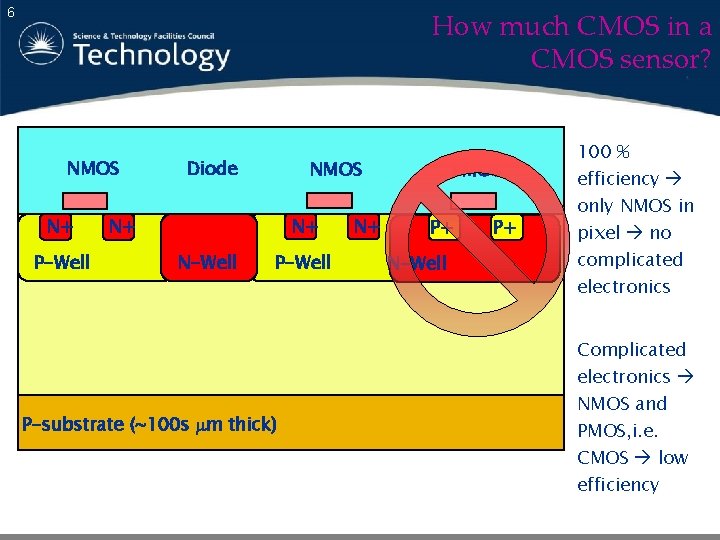
6 How much CMOS in a CMOS sensor? NMOS N+ P-Well Diode NMOS N+ N+ N-Well P-substrate (~100 s mm thick) N+ PMOS P+ N-Well P+ 100 % efficiency only NMOS in pixel no complicated electronics Complicated electronics NMOS and PMOS, i. e. CMOS low efficiency

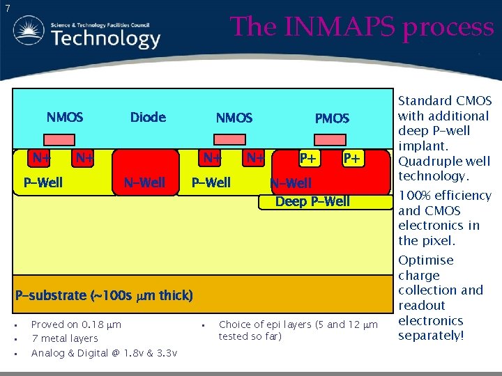
7 The INMAPS process NMOS N+ P-Well Diode NMOS N+ N+ N-Well P-Well N+ PMOS P+ P+ N-Well Deep P-Well P-substrate (~100 s mm thick) • • • Proved on 0. 18 mm 7 metal layers Analog & Digital @ 1. 8 v & 3. 3 v • Choice of epi layers (5 and 12 mm tested so far) Standard CMOS with additional deep P-well implant. Quadruple well technology. 100% efficiency and CMOS electronics in the pixel. Optimise charge collection and readout electronics separately!

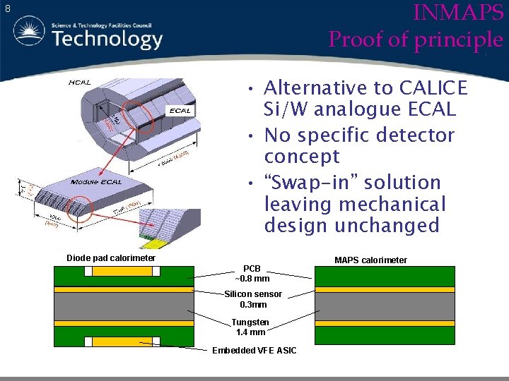
INMAPS Proof of principle 8 • Alternative to CALICE Si/W analogue ECAL • No specific detector concept • “Swap-in” solution leaving mechanical design unchanged Diode pad calorimeter PCB ~0. 8 mm Silicon sensor 0. 3 mm Tungsten 1. 4 mm Embedded VFE ASIC MAPS calorimeter

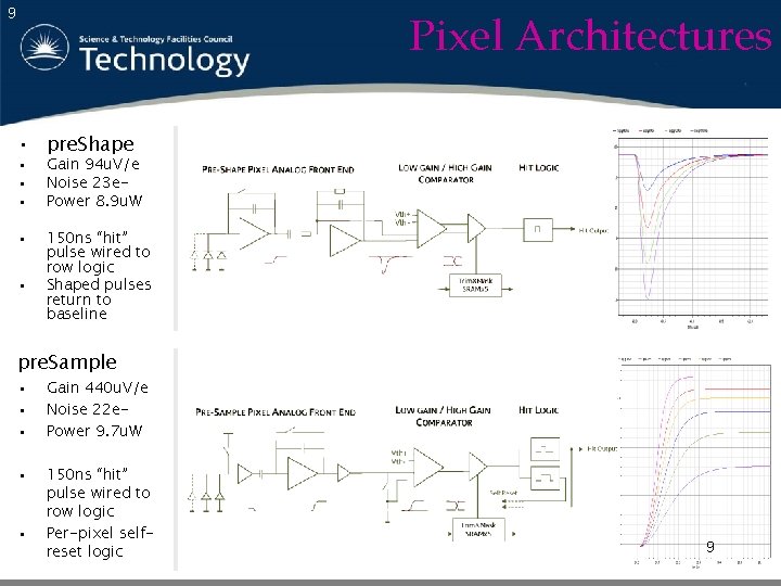
Pixel Architectures 9 • pre. Shape • • • Gain 94 u. V/e Noise 23 e. Power 8. 9 u. W • 150 ns “hit” pulse wired to row logic Shaped pulses return to baseline • pre. Sample • • • Gain 440 u. V/e Noise 22 e. Power 9. 7 u. W • 150 ns “hit” pulse wired to row logic Per-pixel selfreset logic • 9

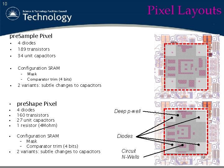
Pixel Layouts 10 pre. Sample Pixel • • • 4 diodes 189 transistors 34 unit capacitors • Configuration SRAM • 2 variants: subtle changes to capacitors – – Mask Comparator trim (4 bits) • pre. Shape Pixel • • 4 diodes 160 transistors 27 unit capacitors 1 resistor (4 Mohm) • Configuration SRAM – Mask – Comparator trim (4 bits) 2 variants: subtle changes to capacitors • Deep p-well Diodes Circuit N-Wells 10

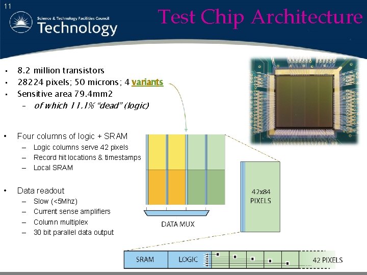
Test Chip Architecture 11 • • • 8. 2 million transistors 28224 pixels; 50 microns; 4 variants Sensitive area 79. 4 mm 2 – of which 11. 1% “dead” (logic) • Four columns of logic + SRAM – Logic columns serve 42 pixels – Record hit locations & timestamps – Local SRAM • Data readout – – Slow (<5 Mhz) Current sense amplifiers Column multiplex 30 bit parallel data output

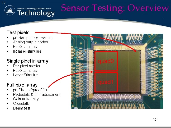
Sensor Testing: Overview 12 Test pixels • • pre. Sample pixel variant Analog output nodes Fe 55 stimulus IR laser stimulus Single pixel in array • • • Per pixel masks Fe 55 stimulus Laser Stimulus Full pixel array • • • quad 0 quad 1 pre. Shape (quad 0/1) Pedestals & trim adjustment Gain uniformity Crosstalk Beam test 12

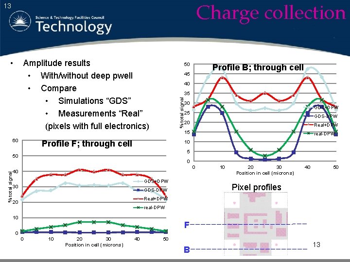
Charge collection 13 • Amplitude results • With/without deep pwell • Compare • Simulations “GDS” • Measurements “Real” (pixels with full electronics) 60 50 40 % total signal 35 30 GDS+DPW 25 GDS-DPW 20 Real+DPW 15 Profile F; through cell real-DPW 10 5 50 % total signal Profile B; through cell 45 0 0 40 GDS+DPW 30 10 20 30 Position in cell (microns) 40 50 Pixel profiles GDS-DPW Real+DPW 20 real-DPW 10 F 0 0 10 20 30 Position in cell (microns) 40 50 B 13

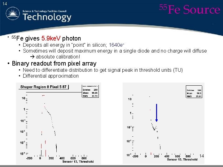
55 Fe 14 • 55 Fe Source gives 5. 9 ke. V photon • Deposits all energy in “point” in silicon; 1640 e− • Sometimes will deposit maximum energy in a single diode and no charge will diffuse absolute calibration! • Binary readout from pixel array • Need to differentiate distribution to get signal peak in threshold units (TU) • Differential approximation 14

15 Conclusions CMOS Active Pixel Sensors are mature for high-end applications Cost-effective solution for large-scale experiments Low noise (< 10 e- rms) Large area: up to 200 mm wafer-scale INMAPS process allows complex in-pixel architectures without degrading the detection performance Evaluating possibility of offering access to the INMAPS process to the community

16 Acknowledgements For the Large Area Sensor (work carried out under the MI-3 Multidimensional Integrated Intelligent Imaging Consortium) A. T. Clark, N. Guerrini, J. P. Crooks, T. Pickering (Rutherford Appleton Laboratory) N. Allinson (University of Sheffield) S. E. Bohndiek (University College London) For the CALICE-MAPS: J. P. Crooks, R. Coath, M. Stanitzki, K. D. Stefanov, M. Tyndel, E. G. Villani (Rutherford Appleton Laboratory) J. A. Ballin, P. D. Dauncey, A. -M. Magnan, M. Noy (Imperial College London) Y. Mikami, N. K. Watson, O. Miller, V. Rajovic, J. A. Wilson (University of Birmingham)