Monolithic pixel detectors with 0 2 mm FDSOI


![Id. Vgs curve with dose Honda (Univ. of Tsukuba) Dose NMOS Vsoi 2=0[V] Vsoi Id. Vgs curve with dose Honda (Univ. of Tsukuba) Dose NMOS Vsoi 2=0[V] Vsoi](https://slidetodoc.com/presentation_image/183b01a51ef6107af1457ae4f62399ca/image-28.jpg)
- Slides: 28

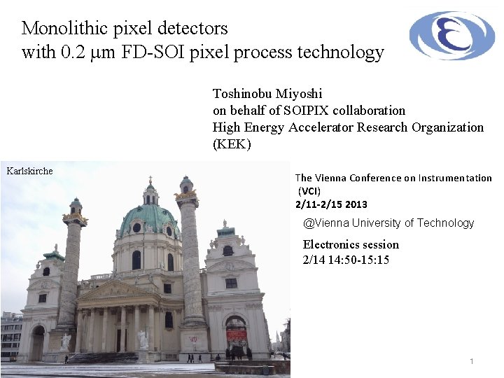
Monolithic pixel detectors with 0. 2 mm FD-SOI pixel process technology Toshinobu Miyoshi on behalf of SOIPIX collaboration High Energy Accelerator Research Organization (KEK) Karlskirche The Vienna Conference on Instrumentation (VCI) 2/11 -2/15 2013 @Vienna University of Technology Electronics session 2/14 14: 50 -15: 15 1

Outline Introduction of SOI detectors Brief review of our activities: measurement of X-rays/charged particles - INTPIX 4, INTPIX 5, XRPIX 1 b, FPIX 1, INTPIX 3 e Main topics: (1) CZn/FZn sensors study (2) Double SOI circuit/sensor study Summary 2

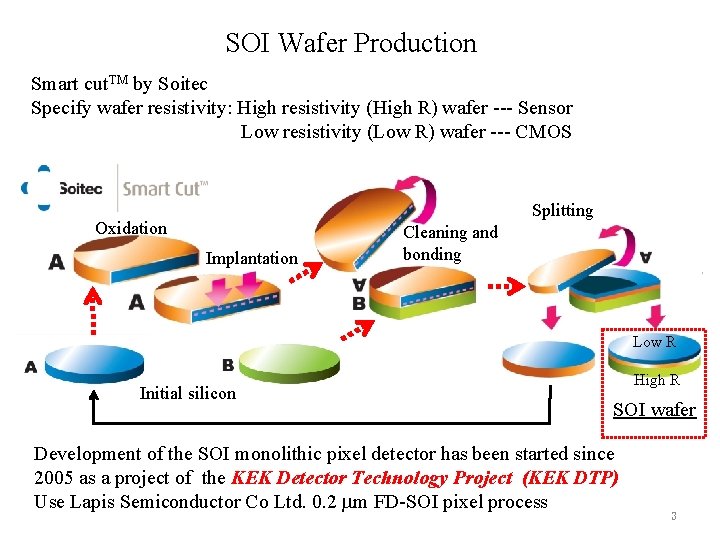
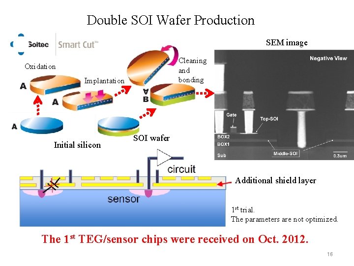
SOI Wafer Production Smart cut. TM by Soitec Specify wafer resistivity: High resistivity (High R) wafer --- Sensor Low resistivity (Low R) wafer --- CMOS Splitting Oxidation Implantation Cleaning and bonding Low R Initial silicon High R SOI wafer Development of the SOI monolithic pixel detector has been started since 2005 as a project of the KEK Detector Technology Project (KEK DTP) Use Lapis Semiconductor Co Ltd. 0. 2 mm FD-SOI pixel process 3

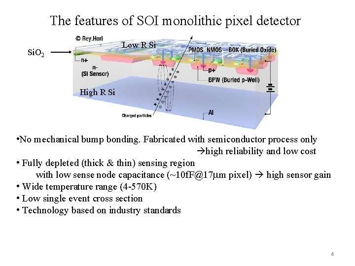
The features of SOI monolithic pixel detector Low R Si Si. O 2 High R Si • No mechanical bump bonding. Fabricated with semiconductor process only high reliability and low cost • Fully depleted (thick & thin) sensing region with low sense node capacitance (~10 f. F@17 mm pixel) high sensor gain • Wide temperature range (4 -570 K) • Low single event cross section • Technology based on industry standards 4

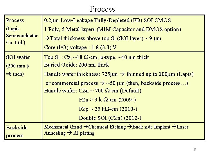
Process 0. 2 mm Low-Leakage Fully-Depleted (FD) SOI CMOS (Lapis Semiconductor Co. Ltd. ) 1 Poly, 5 Metal layers (MIM Capacitor and DMOS option) SOI wafer (200 mm f Top Si : Cz, ~18 -cm, p-type, ~40 nm thick Buried Oxide: 200 nm thick =8 inch) Handle wafer thickness: 725 mm thinned up to 300 mm (Lapis) Total thickness above top Si (SOI layer) ~ 9 mm Core (I/O) voltage : 1. 8 (3. 3) V or commercial process ~50 mm (then, backside process…) Handle wafer: CZn ~ 700 -cm (Default) FZn > 3 k -cm (2009 -) FZp ~ 25 k -cm (2010 -) Double SOI (CZn) (2012 -) Backside process Mechanical Grind Chemical Etching Back side Implant Laser Annealing Al plating 5

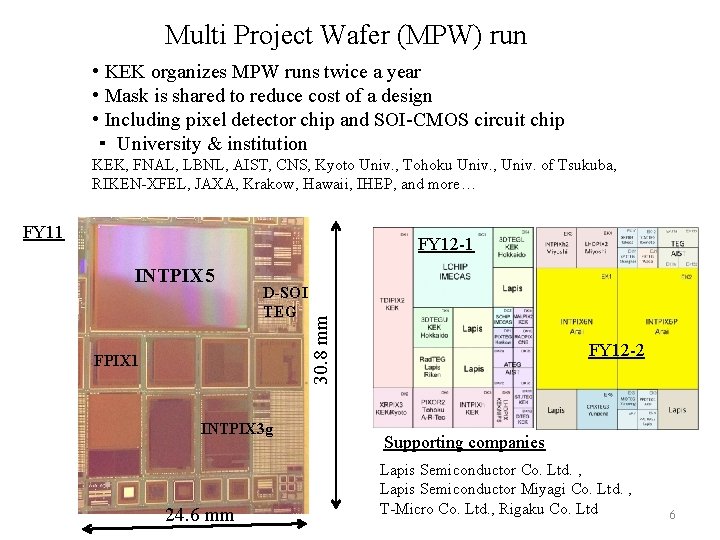
Multi Project Wafer (MPW) run • KEK organizes MPW runs twice a year • Mask is shared to reduce cost of a design • Including pixel detector chip and SOI-CMOS circuit chip ・ University & institution KEK, FNAL, LBNL, AIST, CNS, Kyoto Univ. , Tohoku Univ. , Univ. of Tsukuba, RIKEN-XFEL, JAXA, Krakow, Hawaii, IHEP, and more… FY 11 INTPIX 5 D-SOI TEG FPIX 1 INTPIX 3 g 24. 6 mm 30. 8 mm FY 12 -1 FY 12 -2 Supporting companies Lapis Semiconductor Co. Ltd. , Lapis Semiconductor Miyagi Co. Ltd. , T-Micro Co. Ltd. , Rigaku Co. Ltd 6

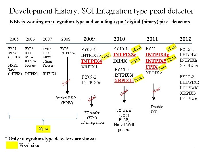
Development history: SOI Integration type pixel detector KEK is working on integration-type and counting-type / digital (binary) pixel detectors 2005 2006 2007 FY 05 MPW (VDEC) FY 06 KEK MPW 0. 15 mm Process FY 07 KEK MPW 0. 2 mm Process PIXEL TEG (INTPIX) INTPIX 1 2008 2009 2010 2011 2012 m FY 10 -1 16 mm FY 11 FY 12 -1 FY 09 -1 18 m LHDPIX INTPIX 3 g INTPIX 3 b 7 mm INTPIX 3 e m 1 DIPIX 14 mm INTPIX 5 12 m INTPIXh INTPIX 4 XRPIX 2 b XRPIX 1 m FPIX m 8 FY 10 -2 XRPIX 2 INTPIX 3 f FY 12 -2 FY 09 -2 m 0 m ! 3 XRPIX 1 b w LHDPIX 2 INTPIX 3 c Ne INTPIXh 2 w! ! e N ew XRPIX 3 N ! Buried P Well w INTPIX 6 Ne FY 08 INTPIX 3 a (BPW) FZ wafer (FZn) 3 D integration 20 mm * Only integration-type detectors are shown Pixel size FZ wafer (FZp) BNW, Nested Well process Double SOI 7

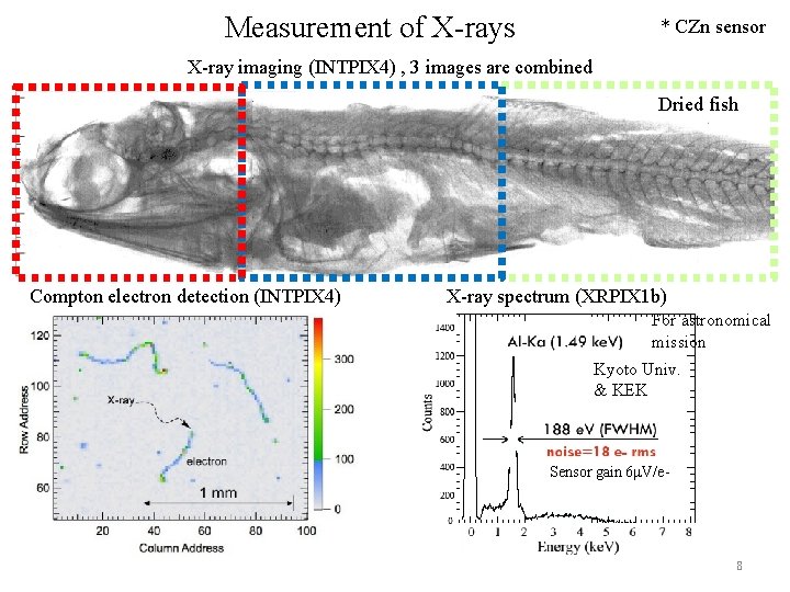
Measurement of X-rays * CZn sensor X-ray imaging (INTPIX 4) , 3 images are combined Dried fish Compton electron detection (INTPIX 4) X-ray spectrum (XRPIX 1 b) For astronomical mission Kyoto Univ. & KEK Sensor gain 6 m. V/e- 8

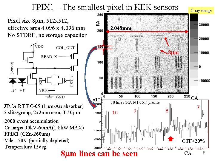
Pixel size 8 mm, 512 x 512, effective area 4. 096 x 4. 096 mm No STORE, no storage capacitor RA FPIX 1 – The smallest pixel in KEK sensors X-ray image 2. 048 mm x 103 JIMA RT RC-05 (1 mm-Au absorber) 3 slits/group, 2 x 2 mm area, 3 -50 mm 2000 event accumulation Cr target 30 k. V-60 m. A(1. 8 k. W MAX) FPIX 1 (CZn-260 um) Vdet=70 V (partially depleted) Temperature 15 deg. CA 10 lines (RA 141 -151) profile 10 9 8 mm lines can be seen 7 8 CTF>20% CA 9

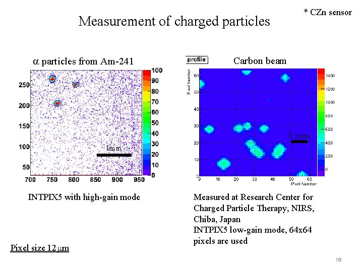
Measurement of charged particles a particles from Am-241 * CZn sensor Carbon beam 0. 1 mm INTPIX 5 with high-gain mode Pixel size 12 mm Measured at Research Center for Charged Particle Therapy, NIRS, Chiba, Japan INTPIX 5 low-gain mode, 64 x 64 pixels are used 10

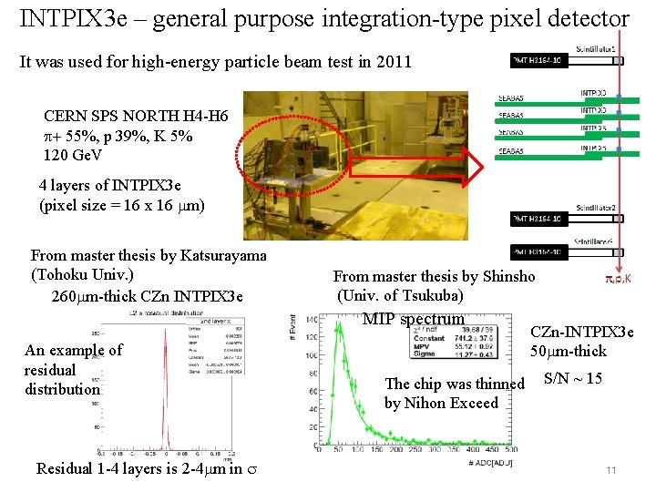
INTPIX 3 e – general purpose integration-type pixel detector It was used for high-energy particle beam test in 2011 CERN SPS NORTH H 4 -H 6 p+ 55%, p 39%, K 5% 120 Ge. V 4 layers of INTPIX 3 e (pixel size = 16 x 16 mm) From master thesis by Katsurayama (Tohoku Univ. ) 260 mm-thick CZn INTPIX 3 e From master thesis by Shinsho (Univ. of Tsukuba) MIP spectrum An example of residual distribution Residual 1 -4 layers is 2 -4 mm in s The chip was thinned by Nihon Exceed CZn-INTPIX 3 e 50 mm-thick S/N ~ 15 11

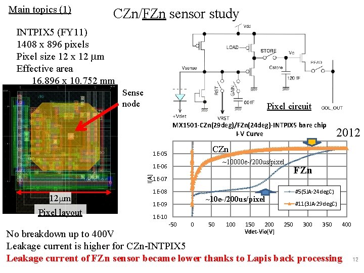
Main topics (1) CZn/FZn sensor study INTPIX 5 (FY 11) 1408 x 896 pixels Pixel size 12 x 12 mm Effective area 16. 896 x 10. 752 mm Sense node Pixel circuit MX 1501 -CZn(29 deg)/FZn(24 deg)-INTPIX 5 bare chip I-V Curve CZn 1 E-05 ~10000 e-/200 us/pixel I[A] 1 E-06 12 mm Pixel layout 2012 1 E-07 1 E-08 #5(5 JA-24 deg. C) ~10 e-/200 us/pixel 1 E-09 FZn #11(3 JA-29 deg. C) 1 E-10 -50 0 50 100 150 200 Vdet-Vio[V] 250 300 350 400 No breakdown up to 400 V Leakage current is higher for CZn-INTPIX 5 Leakage current of FZn sensor became lower thanks to Lapis back processing 12

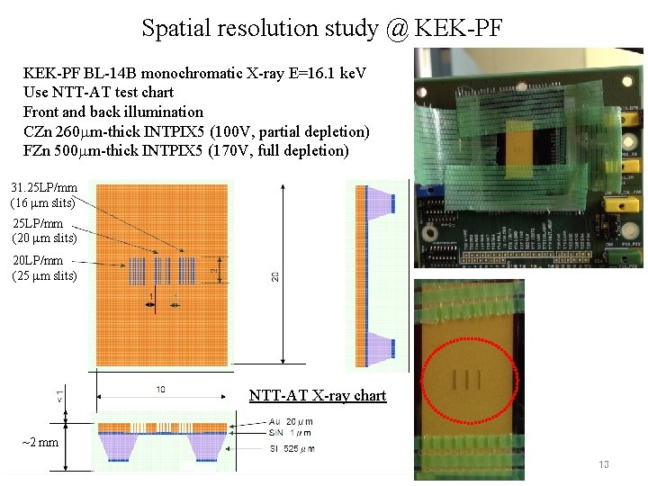
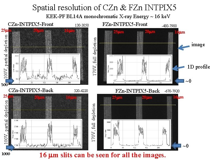
Spatial resolution study @ KEK-PF BL-14 B monochromatic X-ray E=16. 1 ke. V Use NTT-AT test chart Front and back illumination CZn 260 mm-thick INTPIX 5 (100 V, partial depletion) FZn 500 mm-thick INTPIX 5 (170 V, full depletion) 31. 25 LP/mm (16 mm slits) 25 LP/mm (20 mm slits) 20 LP/mm (25 mm slits) NTT-AT X-ray chart ~2 mm 13

Spatial resolution of CZn & FZn INTPIX 5 KEK-PF BL 14 A monochromatic X-ray Energy ~ 16 ke. V CZn-INTPIX 5 -Front FZn-INTPIX 5 -Front 130 -3050 -480 -7900 20 mm 16 mm 25 mm 20 mm 16 mm 170 V, full depletion 100 V, partial depletion 25 mm image 1 D profile ~0 500 CZn-INTPIX 5 -Back 1000 20 mm 16 mm 25 mm -670 -7920 20 mm 16 mm 170 V, full depletion 100 V, partial depletion 25 mm FZn-INTPIX 5 -Back 320 -4220 ~0 16 mm slits can be seen for all the images.

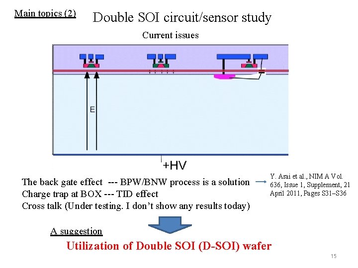
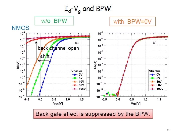
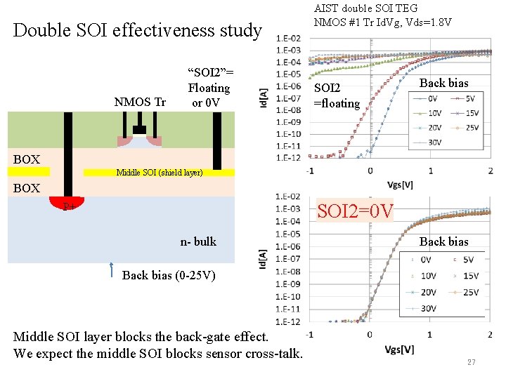
Main topics (2) Double SOI circuit/sensor study Current issues The back gate effect --- BPW/BNW process is a solution Charge trap at BOX --- TID effect Cross talk (Under testing. I don’t show any results today) Y. Arai et al. , NIM A Vol. 636, Issue 1, Supplement, 21 April 2011, Pages S 31–S 36 A suggestion Utilization of Double SOI (D-SOI) wafer 15

Double SOI Wafer Production SEM image Cleaning and bonding Oxidation Implantation Initial silicon SOI wafer Additional shield layer 1 st trial. The parameters are not optimized. The 1 st TEG/sensor chips were received on Oct. 2012. 16

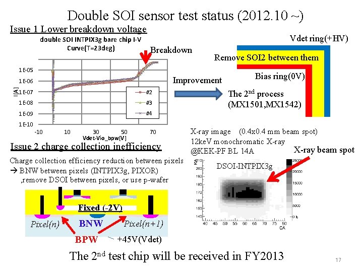
Double SOI sensor test status (2012. 10 ~) Issue 1 Lower breakdown voltage double SOI INTPIX 3 g bare chip I-V Curve(T=23 deg) Vdet ring(+HV) Breakdown Remove SOI 2 between them 1 E-05 Improvement I[A] 1 E-06 1 E-07 #2 1 E-08 #3 1 E-09 #4 1 E-10 10 30 50 Vdet-Vio_bpw[V] 70 Issue 2 charge collection inefficiency Charge collection efficiency reduction between pixels BNW between pixels (INTPIX 3 g, PIXOR) , remove DSOI between pixels, or use p-wafer Bias ring(0 V) The 2 nd process (MX 1501, MX 1542) X-ray image (0. 4 x 0. 4 mm beam spot) 12 ke. V monochromatic X-ray beam spot @KEK-PF BL 14 A DSOI-INTPIX 3 g Fixed (-2 V) Pixel(n) BNW BPW Pixel(n+1) +45 V(Vdet) The 2 nd test chip will be received in FY 2013 17

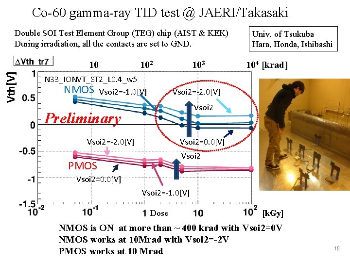
Co-60 gamma-ray TID test @ JAERI/Takasaki Double SOI Test Element Group (TEG) chip (AIST & KEK) During irradiation, all the contacts are set to GND. Vth[V] 10 102 N 33_IONVT_ST 2_L 0. 4_w 5 NMOS Vsoi 2=-1. 0[V] 103 Univ. of Tsukuba Hara, Honda, Ishibashi 104 [krad] Vsoi 2=-2. 0[V] Vsoi 2 Preliminary Vsoi 2=-2. 0[V] Vsoi 2=0. 0[V] Vsoi 2 PMOS Vsoi 2=0. 0[V] Vsoi 2=-1. 0[V] Dose [k. Gy] NMOS is ON at more than ~ 400 krad with Vsoi 2=0 V NMOS works at 10 Mrad with Vsoi 2=-2 V PMOS works at 10 Mrad 18

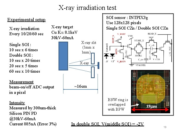
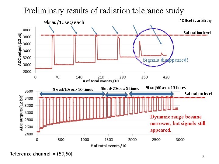
X-ray irradiation test SOI sensor : INTPIX 3 g Use 128 x 128 pixels Single SOI CZn / Double SOI CZn Experimental setup X-ray irradiation Every 10/20/60 sec X-ray target Cu Ka 8. 1 ke. V 30 k. V-60 m. A Single SOI : 10 sec x 6 times Double SOI : 10 sec x 20 times 20 sec x 5 times 60 sec x 10 times Measurement beam-on/off ADC output in a pixel Intensity Measured by 300 um-thick Silicon PIN PD @30 k. V-60 m. A Current 885 n. A (Error 3%) X-ray slit (1 mm x 1 mm) X-ray ~16 cm BNW ring is overlapped with BPW In double SOI, V(middle SOI) = -2 V 18 mm 19

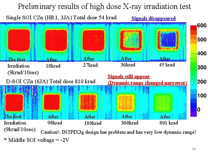
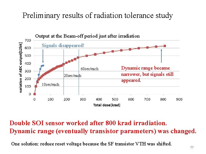
Preliminary results of high dose X-ray irradiation test Single SOI CZn (HR 1, 3 JA) Total dose 54 krad The first Irradiation (9 krad/10 sec) After 18 krad After 27 krad D-SOI CZn (6 JA) Total dose 810 krad The first Irradiation (9 krad/10 sec) After 90 krad After 180 krad Signals disappeared After 36 krad After 45 krad Signals still appear (Dynamic range changed narrower) After 360 krad After 801 krad Caution!: INTPIX 3 g design has problem and has very low dynamic range! * Middle SOI voltage = -2 V 20

Preliminary results of radiation tolerance study *Offset is arbitrary 9 krad/10 sec/each Saturation level Signals disappeared! 9 krad/10 sec x 20 times 9 krad/20 sec x 5 times 9 krad/60 sec x 10 times Saturation level Dynamic range became narrower, but signals still appeared. Reference channel = (50, 50) 21

Preliminary results of radiation tolerance study Output at the Beam-off period just after irradiation Signals disappeared! 60 sec/each 20 sec/each 10 sec/each Dynamic range became narrower, but signals still appeared. Double SOI sensor worked after 800 krad irradiation. Dynamic range (eventually transistor parameters) was changed. One solution: reduce reset voltage because the SF transistor VTH was shifted. 22

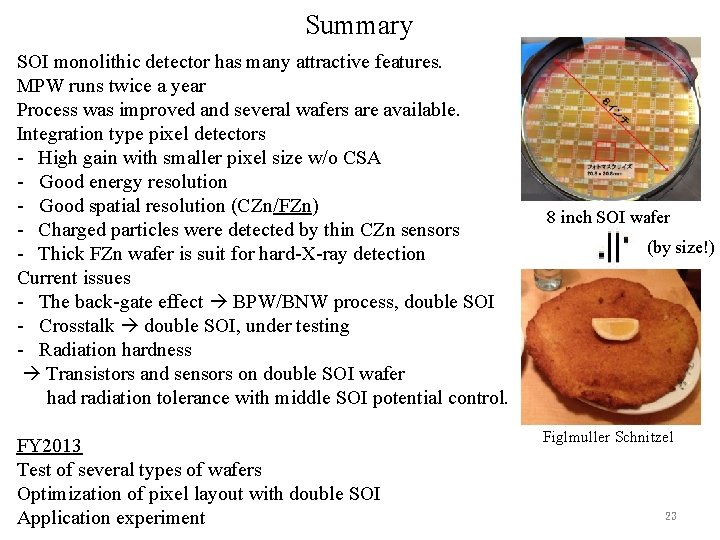
Summary SOI monolithic detector has many attractive features. MPW runs twice a year Process was improved and several wafers are available. Integration type pixel detectors - High gain with smaller pixel size w/o CSA - Good energy resolution - Good spatial resolution (CZn/FZn) - Charged particles were detected by thin CZn sensors - Thick FZn wafer is suit for hard-X-ray detection Current issues - The back-gate effect BPW/BNW process, double SOI - Crosstalk double SOI, under testing - Radiation hardness Transistors and sensors on double SOI wafer had radiation tolerance with middle SOI potential control. FY 2013 Test of several types of wafers Optimization of pixel layout with double SOI Application experiment 8 inch SOI wafer (by size!) Figlmuller Schnitzel 23

SOIPIX Collaboration 2012. 3 ver. KEK : Y. Arai (Project Leader) , Y. Unno, Y. Ikegami, T. Tsuboyama, T. Kohriki, Y. Ikemoto, T. Miyoshi, K. Tauchi, R. Ichimiya, Y. Fujita Grad. Univ. for Adv. Stu. D. Nio, A. Takeda Tsukuba Univ. : K. Hara, T. Ishibashi, Y. Honda Osaka Univ. : K. Hanagaki Tohoku Univ. : H. Yamamoto, Y. Ono, S. Shinoda CNS/Tokyo Univ. : H. Hamagaki, Y. Sekiguchi Kyoto Univ. : T. Tsuru, S. G. Ryu, S. Nakashima Kyoto Univ. of Education: R. Takashima, S. Moritake JAXA/ISAS : H. Ikeda, T. Wada RIKEN X-FEL : T. Hatsui, T. Kudo, M. Omotani, S. Ono Hawaii: G. Varner, M. Cooney, H. Hoedlmoser, J. Kennedy, HB Sahoo LBNL : M. Battaglia, P. Denes, C. Vu, D. Contarato, L. Glesener FNAL : R. Yarema, R. Lipton, G. Deptuch, M. Trimpl, F. F. Khalid Krakow IFJ/AGH: P. Kapusta, I. Ahmed, M. Idzik INFN Padova: D. Bisello, S. Mattiazzo, D. Pantano, P. Giubilato, AIST: M. Ohno, Y. Igarashi, M. Yanagihara, H. Tadokoro, T. Chiba IHEP: Y. Lu Lapis Semiconductor Co. Ltd. : M. Okihara Lapis Semiconductor Miyagi Co. Ltd. : H. Kasai Thank you for your attention! 24

Supplements 25

26

Double SOI effectiveness study NMOS Tr “SOI 2”= Floating or 0 V AIST double SOI TEG NMOS #1 Tr Id. Vg, Vds=1. 8 V SOI 2 =floating Back bias BOX Middle SOI (shield layer) BOX SOI 2=0 V P+ n- bulk Back bias (0 -25 V) Middle SOI layer blocks the back-gate effect. We expect the middle SOI blocks sensor cross-talk. 27
![Id Vgs curve with dose Honda Univ of Tsukuba Dose NMOS Vsoi 20V Vsoi Id. Vgs curve with dose Honda (Univ. of Tsukuba) Dose NMOS Vsoi 2=0[V] Vsoi](https://slidetodoc.com/presentation_image/183b01a51ef6107af1457ae4f62399ca/image-28.jpg)
Id. Vgs curve with dose Honda (Univ. of Tsukuba) Dose NMOS Vsoi 2=0[V] Vsoi 2=-1[V] Vsoi 2=-2[V] N 33_IONVT_ST 2_L 0. 4_w 5 28