High Power Impulse Magnetron Sputtering High Power Pulse
- Slides: 15

High Power Impulse Magnetron Sputtering / High Power Pulse Magnetron Sputtering (Hi. PIMS/HPPMS) Technology, applications and possibilities Anna Gustafsson

Overview • Introduction into Magnetron Sputtering • Hi. PIMS • Physical processes • Film properties • Applications • Pro’s and Con’s • The Hi. PIMS Power Supply • Summary & Outlook 2

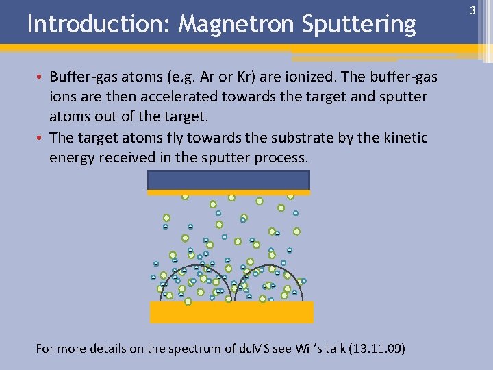
Introduction: Magnetron Sputtering • Buffer-gas atoms (e. g. Ar or Kr) are ionized. The buffer-gas ions are then accelerated towards the target and sputter atoms out of the target. • The target atoms fly towards the substrate by the kinetic energy received in the sputter process. - - - - - -- - - - -- - For more details on the spectrum of dc. MS see Wil’s talk (13. 11. 09) 3

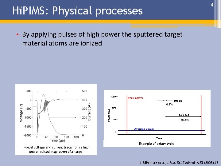
Hi. PIMS: Physical processes 4 • By applying pulses of high power the sputtered target material atoms are ionized Typical voltage and current trace from a high power pulsed magnetron discharge. Example of a duty cycle. J. Böhlmark et al. , J. Vac. Sci. Technol. A 23 (2005) 18

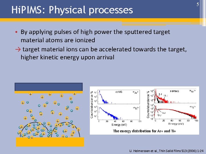
Hi. PIMS: Physical processes 5 • By applying pulses of high power the sputtered target material atoms are ionized → target material ions can be accelerated towards the target, higher kinetic energy upon arrival + + - + +- -+ -+ + - - +- -+ + --+ +- -+ --+- -+ - - + - + +- - + +- ++ + +- +- -+ -- +- +- -+ + + +-- - + The energy distribution for Ar+ and Ti+ U. Helmersson et al. , Thin Solid Films 513 (2006) 1 -24

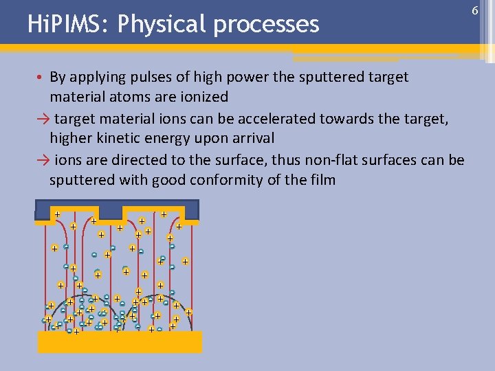
Hi. PIMS: Physical processes • By applying pulses of high power the sputtered target material atoms are ionized → target material ions can be accelerated towards the target, higher kinetic energy upon arrival → ions are directed to the surface, thus non-flat surfaces can be sputtered with good conformity of the film + + + ++ + + - +- + +- - + -+ +- +- + + ++ + - + + +- +- -+ + + -+ -- +- -+ +- -- -+ + + + - +- - --+ -+ - - - + -- ++- + + 6

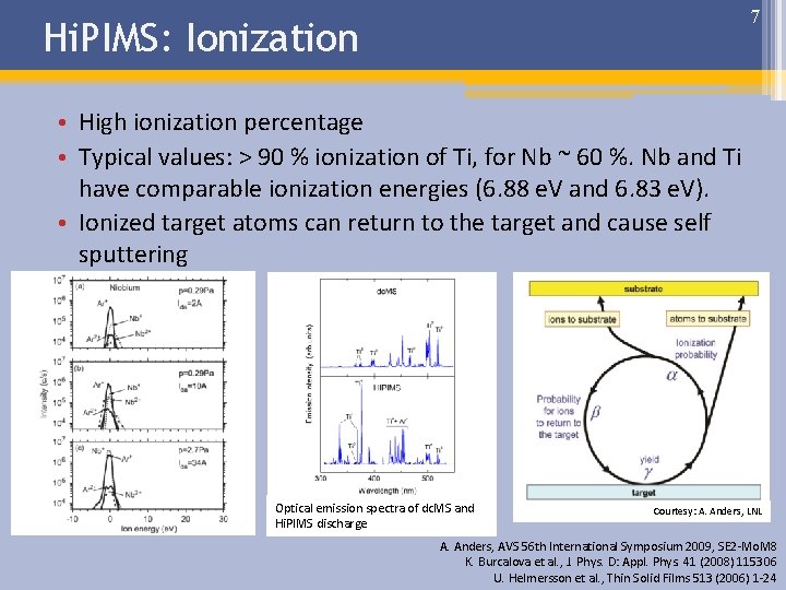
7 Hi. PIMS: Ionization • High ionization percentage • Typical values: > 90 % ionization of Ti, for Nb ~ 60 %. Nb and Ti have comparable ionization energies (6. 88 e. V and 6. 83 e. V). • Ionized target atoms can return to the target and cause self sputtering Optical emission spectra of dc. MS and Hi. PIMS discharge Courtesy: A. Anders, LNL A. Anders, AVS 56 th International Symposium 2009, SE 2 -Mo. M 8 K. Burcalova et al. , J. Phys. D: Appl. Phys. 41 (2008) 115306 U. Helmersson et al. , Thin Solid Films 513 (2006) 1 -24

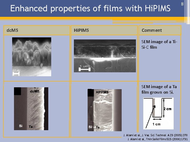
Enhanced properties of films with Hi. PIMS dc. MS Hi. PIMS 8 Comment SEM image of a Ti. Si-C film SEM image of a Ta film grown on Si. J. Alami et al. , J. Vac. Sci. Technol. A 23 (2005) 278 J. Alami et al. , Thin Solid Films 515 (2006) 1731

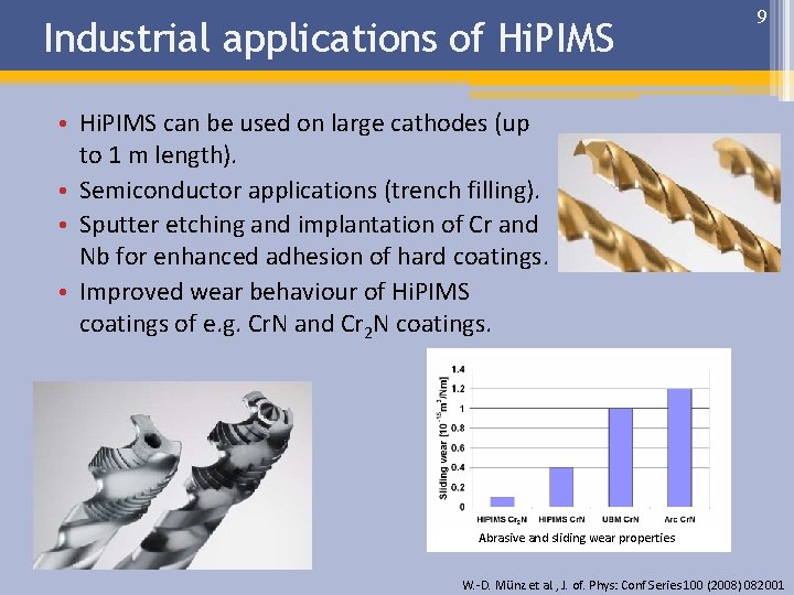
Industrial applications of Hi. PIMS 9 • Hi. PIMS can be used on large cathodes (up to 1 m length). • Semiconductor applications (trench filling). • Sputter etching and implantation of Cr and Nb for enhanced adhesion of hard coatings. • Improved wear behaviour of Hi. PIMS coatings of e. g. Cr. N and Cr 2 N coatings. Abrasive and sliding wear properties W. -D. Münz et al. , J. of. Phys: Conf Series 100 (2008) 082001

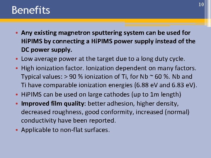
Benefits • Any existing magnetron sputtering system can be used for Hi. PIMS by connecting a Hi. PIMS power supply instead of the DC power supply. • Low average power at the target due to a long duty cycle. • High ionization factor. Ionization dependent on many factors. Typical values: > 90 % ionization of Ti, for Nb ~ 60 %. Nb and Ti have comparable ionization energies (6. 88 e. V and 6. 83 e. V). • Hi. PIMS can be used on large cathodes (up to 1 m length) • Improved film quality: better adhesion, higher density, decreased roughness, good conformity, increased (normal) conductivity have been reported. • Applicable to non-flat surfaces. 10

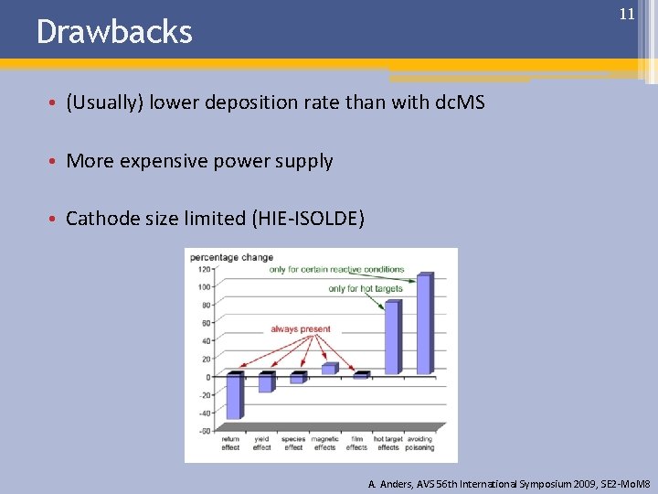
11 Drawbacks • (Usually) lower deposition rate than with dc. MS • More expensive power supply • Cathode size limited (HIE-ISOLDE) A. Anders, AVS 56 th International Symposium 2009, SE 2 -Mo. M 8

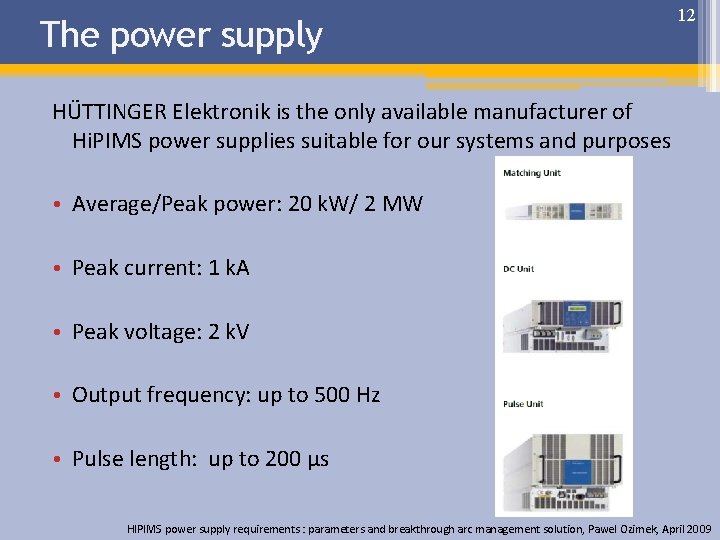
The power supply 12 HÜTTINGER Elektronik is the only available manufacturer of Hi. PIMS power supplies suitable for our systems and purposes • Average/Peak power: 20 k. W/ 2 MW • Peak current: 1 k. A • Peak voltage: 2 k. V • Output frequency: up to 500 Hz • Pulse length: up to 200 μs HIPIMS power supply requirements : parameters and breakthrough arc management solution, Pawel Ozimek, April 2009

Outlook • Establish a Hi. PIMS coating system for small samples by use of the DMS in Building 101, understanding the different parameters and optimize the system. • Produce Nb films on Cu samples to investigate superconducting properties as well as RF properties. • Investigations of the so-called Q-drop mechanism to possibly improve the performance of Nb film cavities by this new sputtering technique. • Tests of the Hi. PIMS PS on the HIE-ISOLDE coating system. Cathode is cylindrical and much bigger surface, thus the feasibility has to be tested. 13

Summary • Hi. PIMS will not replace the conventional DC method, due to it’s lower deposition rate and expensive power supplies. • Enhanced film properties gives an important complement to the existing systems. • Superconducting properties of Nb films have hardly been investigated yet, but the enhanced film properties give a promising hint of improvements. • The community is very convinced that Hi. PIMS is “the way to go” 14

Thanks for your attention References • J. Alami et al. , J. Vac. Sci. Technol. A 23 (2005) 278 • J. Alami et al. , Thin Solid Films 515 (2006) 1731 • A. Anders, AVS 56 th International Symposium 2009, SE 2 -Mo. M 8 • K. Burcalova et al. , J. Phys. D: Appl. Phys. 41 (2008) 115306 • J. Böhlmark et al. , J. Vac. Sci. Technol. A 23 (2005) 18 • V. Kouznetsov et al. , Surf. Coat. Technol. 122 (1999) 290 • W. -D. Münz et al. , J. of. Phys: Conf Series 100 (2008) 082001 • HIPIMS power supply requirements : parameters and breakthrough arc management solution Pawel Ozimek, April 2009 Review on Ionized Physical Vapor Deposition (IPVD): • U. Helmersson et al. , Thin Solid Films 513 (2006) 1 -24 15