Uses of Plasmas in Deposition Sputtering Outline Additive

- Slides: 22


Uses of Plasmas in Deposition: Sputtering

Outline • • • Additive processes Sputtering Basic Theory Types of sputtering Applications of sputtering

Additive processes • These are what are termed deposition processes--- adding a thin film of a material • There are many types; e. g. , evaporation, sputtering, chemical vapor deposition, plasma enhanced deposition, atomic layer deposition.

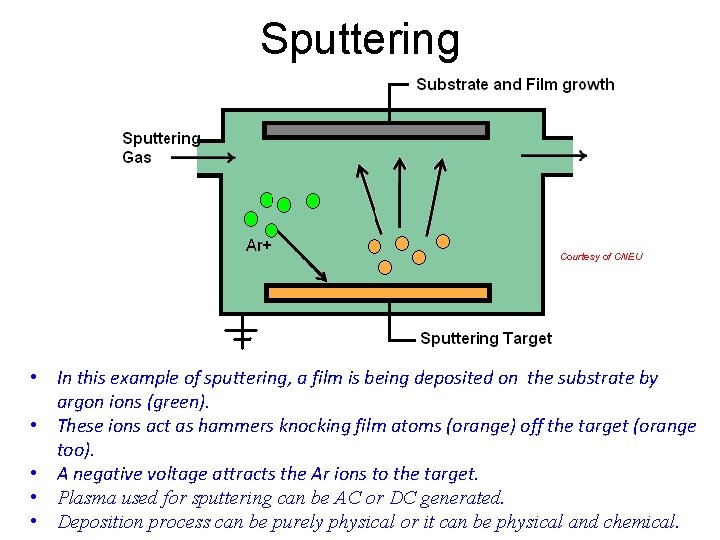
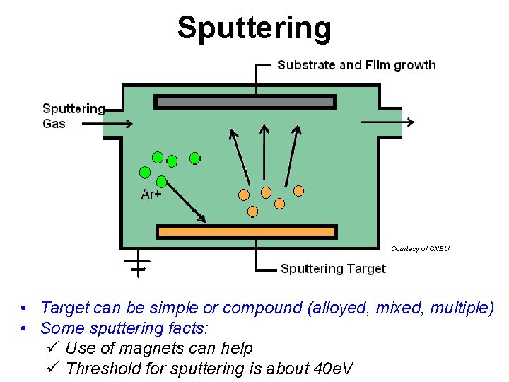
Sputtering Courtesy of CNEU • In this example of sputtering, a film is being deposited on the substrate by argon ions (green). • These ions act as hammers knocking film atoms (orange) off the target (orange too). • A negative voltage attracts the Ar ions to the target. • Plasma used for sputtering can be AC or DC generated. • Deposition process can be purely physical or it can be physical and chemical.

Reactive Sputter Deposition • Add reactive gas to chamber during deposition (evaporation or sputtering) oxygen, nitrogen • Chemical reaction takes place on substrate and target can poison target if chemical reactions are faster than sputter rate • Adjust reactive gas flow to get good stoichiometry without incorporating excess gas into film

Sputtering Courtesy of CNEU • Target can be simple or compound (alloyed, mixed, multiple) • Some sputtering facts: ü Use of magnets can help ü Threshold for sputtering is about 40 e. V

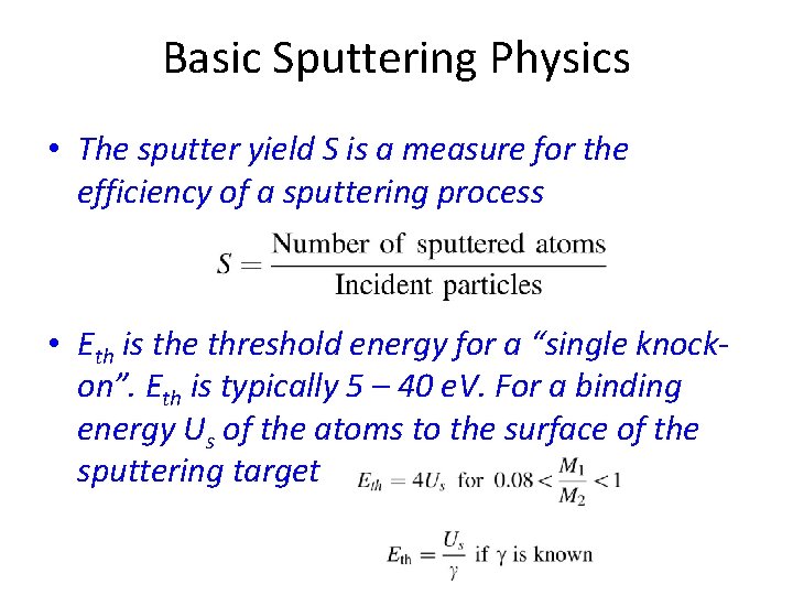
Basic Sputtering Physics • The sputter yield S is a measure for the efficiency of a sputtering process • Eth is the threshold energy for a “single knockon”. Eth is typically 5 – 40 e. V. For a binding energy Us of the atoms to the surface of the sputtering target

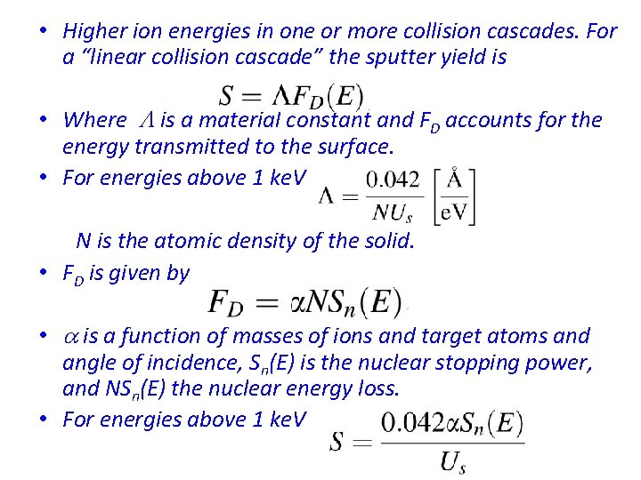
• Higher ion energies in one or more collision cascades. For a “linear collision cascade” the sputter yield is • Where L is a material constant and FD accounts for the energy transmitted to the surface. • For energies above 1 ke. V N is the atomic density of the solid. • FD is given by • a is a function of masses of ions and target atoms and angle of incidence, Sn(E) is the nuclear stopping power, and NSn(E) the nuclear energy loss. • For energies above 1 ke. V

Summary: Basic Sputtering Techniques • DC (diode) • RF (radio frequency) • magnetron

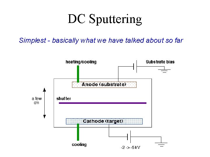
DC Sputtering Simplest - basically what we have talked about so far

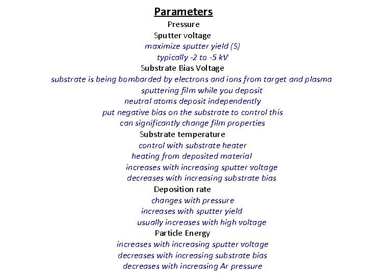
Parameters Pressure Sputter voltage maximize sputter yield (S) typically -2 to -5 k. V Substrate Bias Voltage substrate is being bombarded by electrons and ions from target and plasma sputtering film while you deposit neutral atoms deposit independently put negative bias on the substrate to control this can significantly change film properties Substrate temperature control with substrate heater heating from deposited material increases with increasing sputter voltage decreases with increasing substrate bias Deposition rate changes with pressure increases with sputter yield usually increases with high voltage Particle Energy increases with increasing sputter voltage decreases with increasing substrate bias decreases with increasing Ar pressure

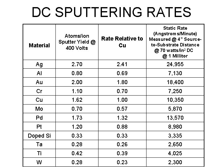
DC SPUTTERING RATES Material Atoms/ion Rate Relative to Sputter Yield @ Cu 400 Volts Static Rate (Angstroms/Minute) Measured @ 4” Sourceto-Substrate Distance @ 70 watts/in 2 DC @ 1 Millitor Ag 2. 70 2. 41 24, 955 Al 0. 80 0. 69 7, 130 Au 2. 00 1. 80 18, 400 Cr 1. 10 0. 70 7, 250 Cu 1. 62 1. 00 10, 350 Mo 0. 70 0. 57 5, 870 Pd 1. 73 1. 32 13, 570 Pt 1. 20 0. 88 8, 980 Doped Si 0. 33 3, 335 Ta 0. 28 0. 26 2, 650 Ti 0. 42 0. 39 4, 025 W 0. 28 0. 23 2, 300

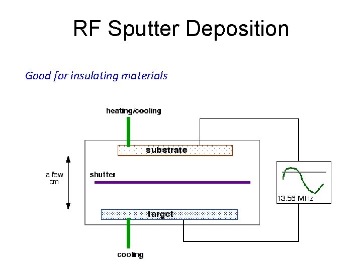
RF Sputter Deposition Good for insulating materials

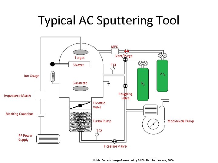
Typical AC Sputtering Tool MFC Vent/Purge Target Shutter TC 1 Ar 2 Ion Gauge Substrate N 2 Roughing Valve Impedance Match Throttle Valve Blocking Capacitor Turbo Pump Mechanical Pump TC 2 RF Power Supply Foreline Valve Public Domain: Image Generated by CNEU Staff for free use, 2009

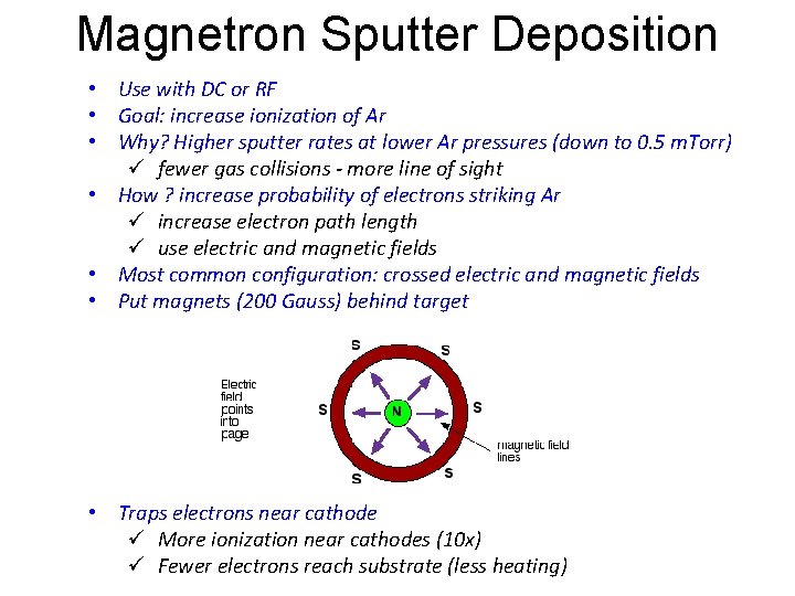
Magnetron Sputter Deposition • Use with DC or RF • Goal: increase ionization of Ar • Why? Higher sputter rates at lower Ar pressures (down to 0. 5 m. Torr) ü fewer gas collisions - more line of sight • How ? increase probability of electrons striking Ar ü increase electron path length ü use electric and magnetic fields • Most common configuration: crossed electric and magnetic fields • Put magnets (200 Gauss) behind target • Traps electrons near cathode ü More ionization near cathodes (10 x) ü Fewer electrons reach substrate (less heating)

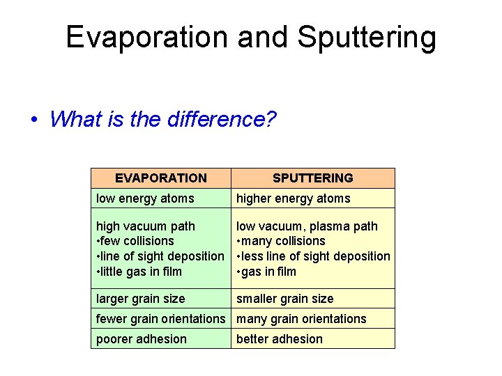
Evaporation and Sputtering • What is the difference? EVAPORATION SPUTTERING low energy atoms higher energy atoms high vacuum path • few collisions • line of sight deposition • little gas in film low vacuum, plasma path • many collisions • less line of sight deposition • gas in film larger grain size smaller grain size fewer grain orientations many grain orientations poorer adhesion better adhesion

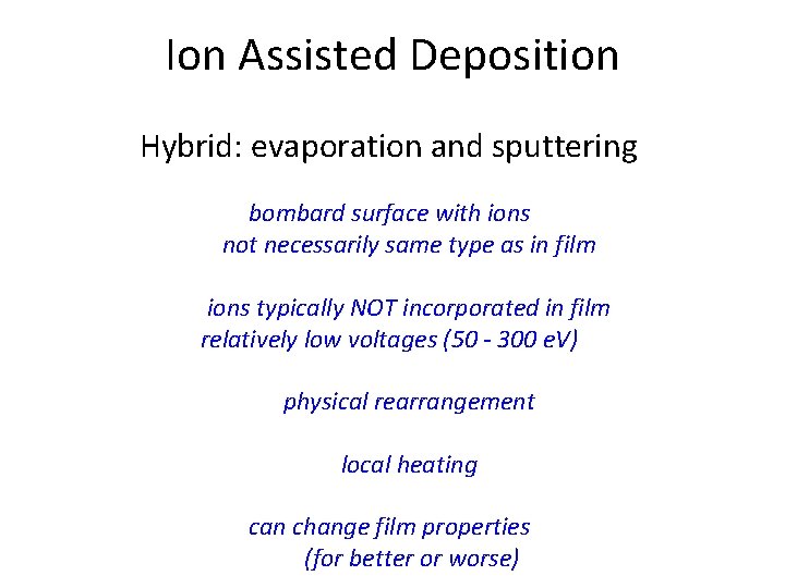
Ion Assisted Deposition Hybrid: evaporation and sputtering bombard surface with ions not necessarily same type as in film ions typically NOT incorporated in film relatively low voltages (50 - 300 e. V) physical rearrangement local heating can change film properties (for better or worse)

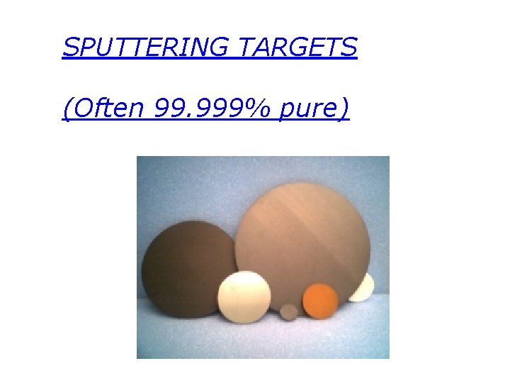
SPUTTERING TARGETS (Often 99. 999% pure)

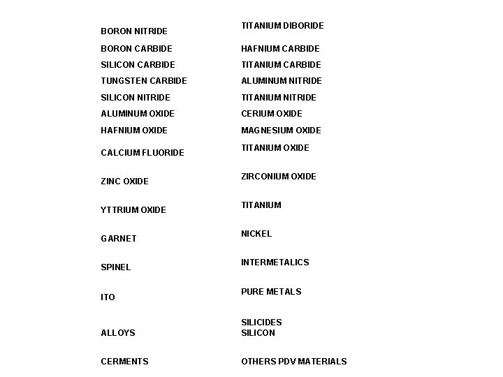
BORON NITRIDE TITANIUM DIBORIDE BORON CARBIDE HAFNIUM CARBIDE SILICON CARBIDE TITANIUM CARBIDE TUNGSTEN CARBIDE ALUMINUM NITRIDE SILICON NITRIDE TITANIUM NITRIDE ALUMINUM OXIDE CERIUM OXIDE HAFNIUM OXIDE MAGNESIUM OXIDE CALCIUM FLUORIDE ZINC OXIDE YTTRIUM OXIDE GARNET SPINEL ITO TITANIUM OXIDE ZIRCONIUM OXIDE TITANIUM NICKEL INTERMETALICS PURE METALS ALLOYS SILICIDES SILICON CERMENTS OTHERS PDV MATERIALS

Uses of Sputtering • Depositing thin films for many, many applications • Can deposit metals, semiconductors, and insulators • Large areas • High deposition rates

Summary • Very versatile technique • Can be used to deposit many types of films • High deposition rate • Can cause damage