Hierarchical Physical Design Methodology for MultiMillion Gate Chips




- Slides: 17

Hierarchical Physical Design Methodology for Multi-Million Gate Chips Session 11 Wei-Jin Dai

Overview • Introduction • Challenges of hierarchical design • Hierarchical methodology – Full chip physical prototyping • Performance data • Summary 2

Introduction • As chip size and complexity grow, hierarchical design approach is necessary • During last 12 months, there is a big increase in the number of chips designed with hierarchical approach • The advantages of hierarchical approach is divide-and-conquer 3

The Challenges • How to get full-chip (10 million gates+) physical reality early on to identify potential problems? • How to have convergence process to reach design closure from beginning to end? • How to achieve die utilization similar to “flat” approach? • How to achieve clock speed and skews similar to “flat” approach? • How to automatically generate optimal pin assignments for each module? • How to automatically come up with realistic timing budgets for each module? • How to achieve top level timing/signal integrity closure? 4

Creating the Physical Prototype Flat Full-Chip Delivers an Accurate Physical Prototype • Full-chip flat prototype delivers the complete physical, timing, clock and power data – Eliminates the guessing of the traditional block-based approaches • Drives the partitioning in manageable blocks 5

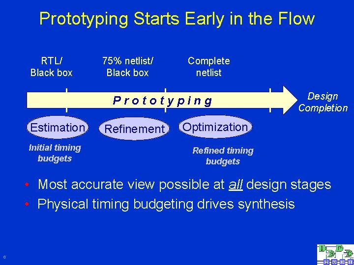
Prototyping Starts Early in the Flow RTL/ Black box 75% netlist/ Black box Complete netlist Prototyping Estimation Initial timing budgets Refinement Design Completion Optimization Refined timing budgets • Most accurate view possible at all design stages • Physical timing budgeting drives synthesis 6

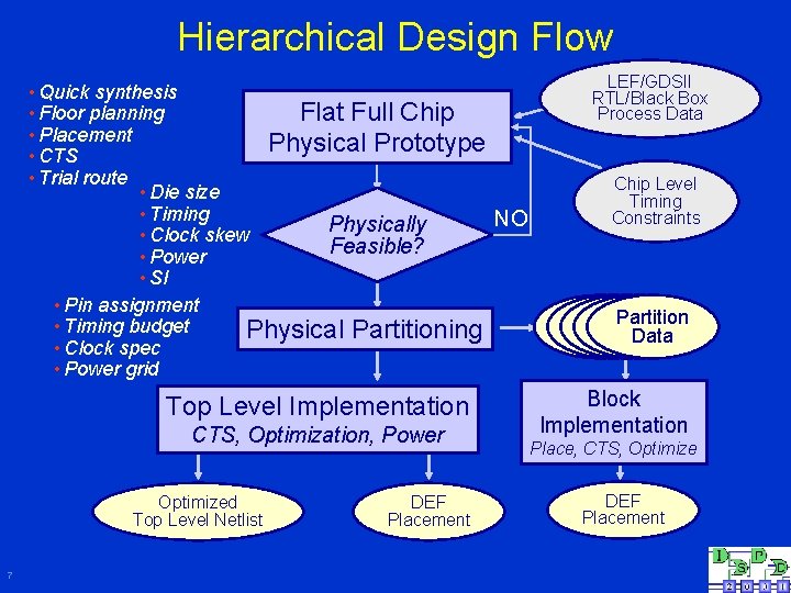
Hierarchical Design Flow • Quick synthesis • Floor planning Flat Full Chip • Placement Physical Prototype • CTS • Trial route • Die size • Timing NO Physically • Clock skew Feasible? • Power • SI • Pin assignment • Timing budget Physical Partitioning • Clock spec • Power grid Top Level Implementation CTS, Optimization, Power Optimized Top Level Netlist 7 DEF Placement LEF/GDSII RTL/Black Box Process Data Chip Level Timing Constraints Partition Partition Data Data Block Implementation Place, CTS, Optimize DEF Placement

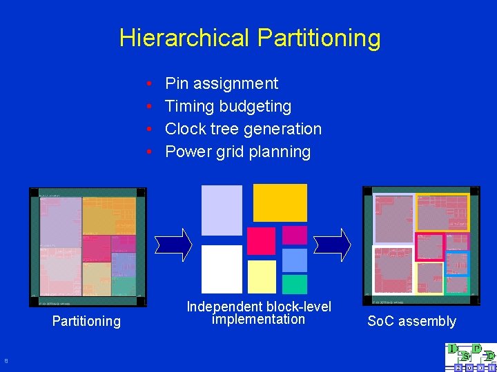
Hierarchical Partitioning • • Partitioning 8 Pin assignment Timing budgeting Clock tree generation Power grid planning Independent block-level implementation So. C assembly

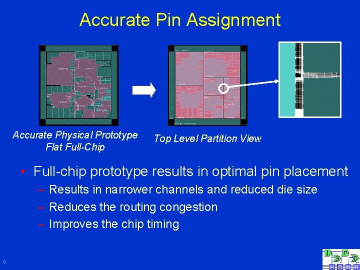
Accurate Pin Assignment Accurate Physical Prototype Flat Full-Chip Top Level Partition View • Full-chip prototype results in optimal pin placement – Results in narrower channels and reduced die size – Reduces the routing congestion – Improves the chip timing 9

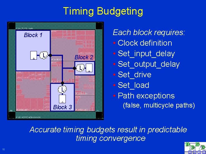
Timing Budgeting Block 1 L Block 2 L L Block 3 Each block requires: • Clock definition • Set_input_delay • Set_output_delay • Set_drive • Set_load • Path exceptions (false, multicycle paths) Accurate timing budgets result in predictable timing convergence 10

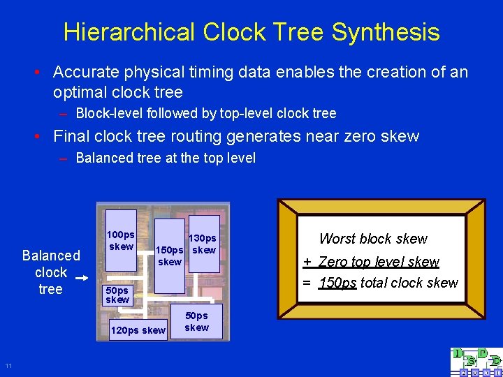
Hierarchical Clock Tree Synthesis • Accurate physical timing data enables the creation of an optimal clock tree – Block-level followed by top-level clock tree • Final clock tree routing generates near zero skew – Balanced tree at the top level Balanced clock tree 100 ps skew 130 ps 150 ps skew 120 ps skew 11 50 ps skew Worst block skew + Zero top level skew = 150 ps total clock skew

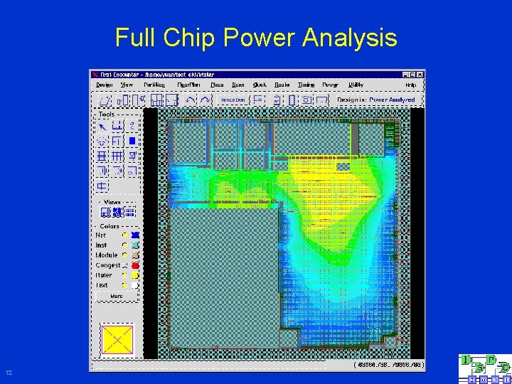
Full Chip Power Analysis 12

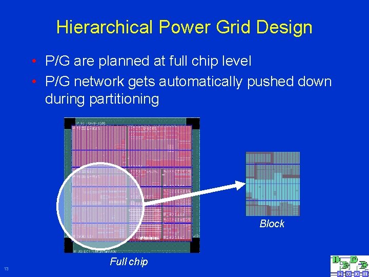
Hierarchical Power Grid Design • P/G are planned at full chip level • P/G network gets automatically pushed down during partitioning Block 13 Full chip

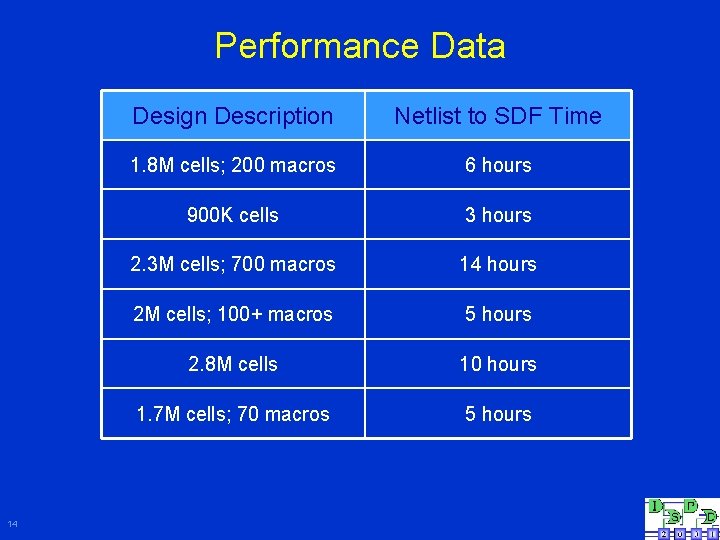
Performance Data 14 Design Description Netlist to SDF Time 1. 8 M cells; 200 macros 6 hours 900 K cells 3 hours 2. 3 M cells; 700 macros 14 hours 2 M cells; 100+ macros 5 hours 2. 8 M cells 10 hours 1. 7 M cells; 70 macros 5 hours

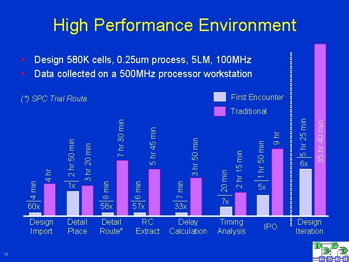
High Performance Environment • Design 580 K cells, 0. 25 um process, 5 LM, 100 MHz • Data collected on a 500 MHz processor workstation First Encounter (*) SPC Trial Route Design Import 15 Detail Place 57 x 33 x Detail Route* RC Extract Delay Calculation 6 x 35 hr 40 min 5 hr 25 min 9 hr 1 hr 50 min 2 hr 15 min 56 x 20 min 7 min 3 hr 50 min 5 hr 45 min 7 hr 30 min 60 x 8 min 1 x 3 hr 20 min 2 hr 50 min 4 hr 4 min Traditional 5 x 7 x Timing Analysis IPO Design Iteration

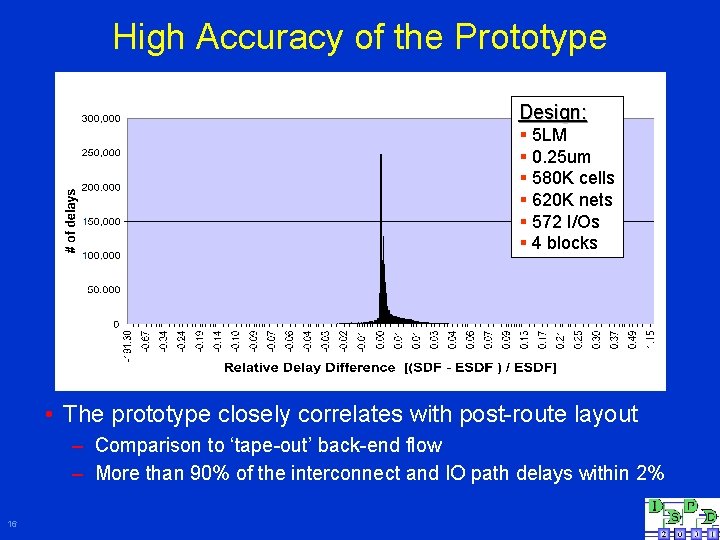
High Accuracy of the Prototype Design: § 5 LM § 0. 25 um § 580 K cells § 620 K nets § 572 I/Os § 4 blocks • The prototype closely correlates with post-route layout – Comparison to ‘tape-out’ back-end flow – More than 90% of the interconnect and IO path delays within 2% 16

Summary So. C Hierarchical Methodology • Build a full-chip physical prototype early on – Start at RTL – Identify problems early • Achieve design closure before partitioning – – Close full-chip timing Optimize die size Meet power requirements Resolve signal integrity issues • Maintain the design closure throughout the design process 17