Epson Piezoelectric Colour Inkjet Printer ECE 434 Presentation

- Slides: 19
Epson Piezoelectric Colour Inkjet Printer ECE 434 Presentation Aurélie Barras Jeff Emmett Hannes Rose
Outline Introduction Product Definition Operating Principle Fabrication and Manufacture Packaging Principles Signal Transduction Technique Future Applications
Introduction Origin of piezoelectric effect: atomic arrangements Lack a center of inversion symmetry able to create internal electric polarization Piezoelectric materials: quartz, tourmaline, gallium orthophosphate, crystals of the CGG group, piezoelectric ceramics Useful for fast-response applications and for sensing or generating vibrations
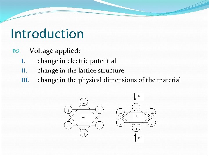
Introduction Voltage applied: I. III. change in electric potential change in the lattice structure change in the physical dimensions of the material F + + +- - + + - - + F
Product Definition Applications: reach from high end products for special purposes to very cheap devices for private households Desired objectives: speed, cost effectiveness, high print resolution and manufacturability Epson patent: Use of piezoelectric elements to expel ink droplets from the print head one drop at a time
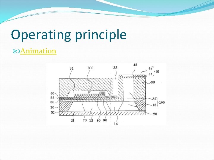
Operating principle Animation
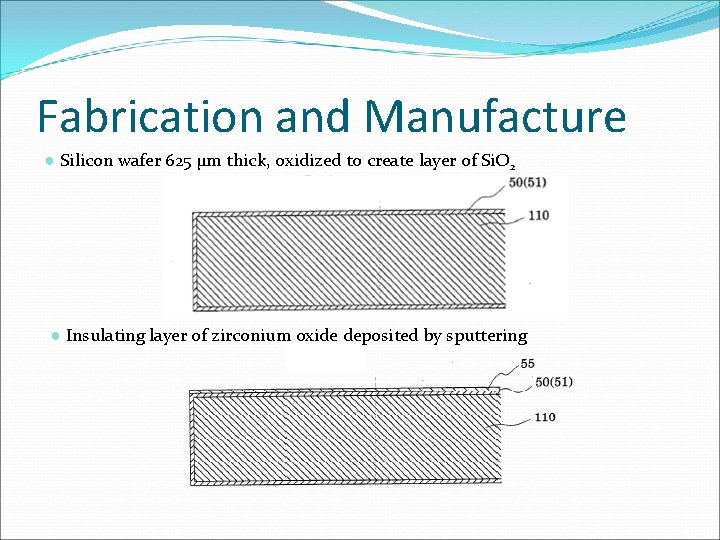
Fabrication and Manufacture ● Silicon wafer 625 µm thick, oxidized to create layer of Si. O 2 ● Insulating layer of zirconium oxide deposited by sputtering
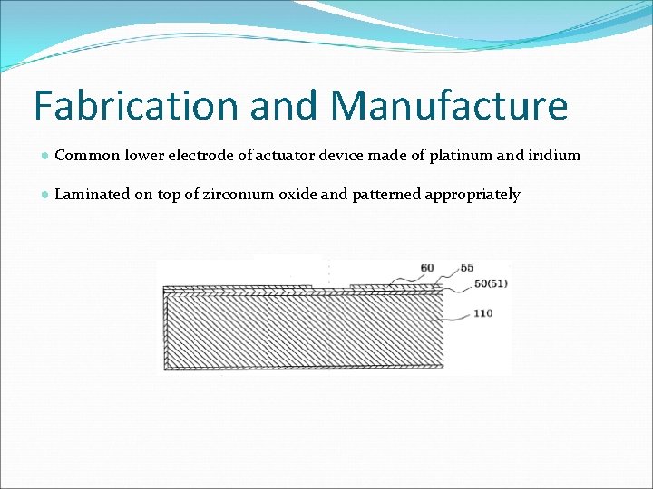
Fabrication and Manufacture ● Common lower electrode of actuator device made of platinum and iridium ● Laminated on top of zirconium oxide and patterned appropriately
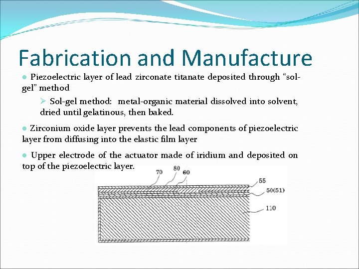
Fabrication and Manufacture ● Piezoelectric layer of lead zirconate titanate deposited through “solgel” method Ø Sol-gel method: metal-organic material dissolved into solvent, dried until gelatinous, then baked. ● Zirconium oxide layer prevents the lead components of piezoelectric layer from diffusing into the elastic film layer ● Upper electrode of the actuator made of iridium and deposited on top of the piezoelectric layer.
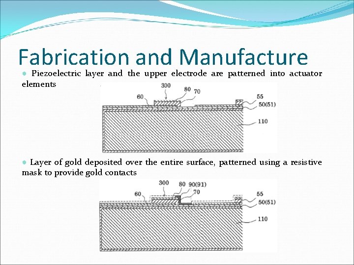
Fabrication and Manufacture ● Piezoelectric layer and the upper electrode are patterned into actuator elements ● Layer of gold deposited over the entire surface, patterned using a resistive mask to provide gold contacts
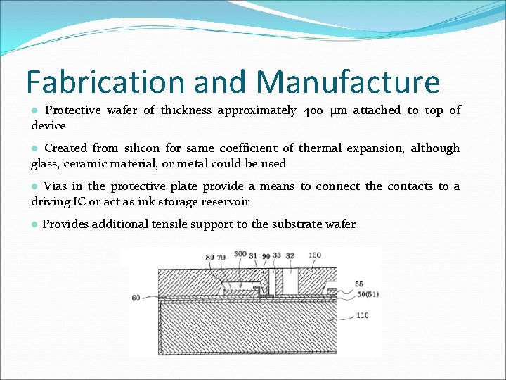
Fabrication and Manufacture ● Protective wafer of thickness approximately 400 µm attached to top of device ● Created from silicon for same coefficient of thermal expansion, although glass, ceramic material, or metal could be used ● Vias in the protective plate provide a means to connect the contacts to a driving IC or act as ink storage reservoir ● Provides additional tensile support to the substrate wafer
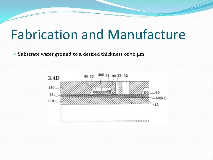
Fabrication and Manufacture ● Substrate wafer ground to a desired thickness of 70 µm
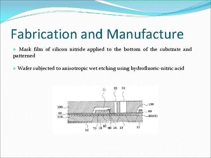
Fabrication and Manufacture ● Mask film of silicon nitride applied to the bottom of the substrate and patterned ● Wafer subjected to anisotropic wet etching using hydrofluoric-nitric acid
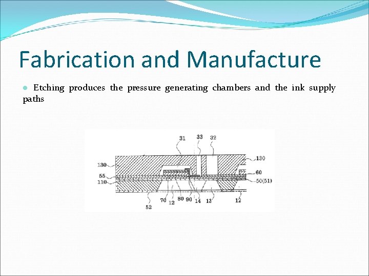
Fabrication and Manufacture ● Etching produces the pressure generating chambers and the ink supply paths
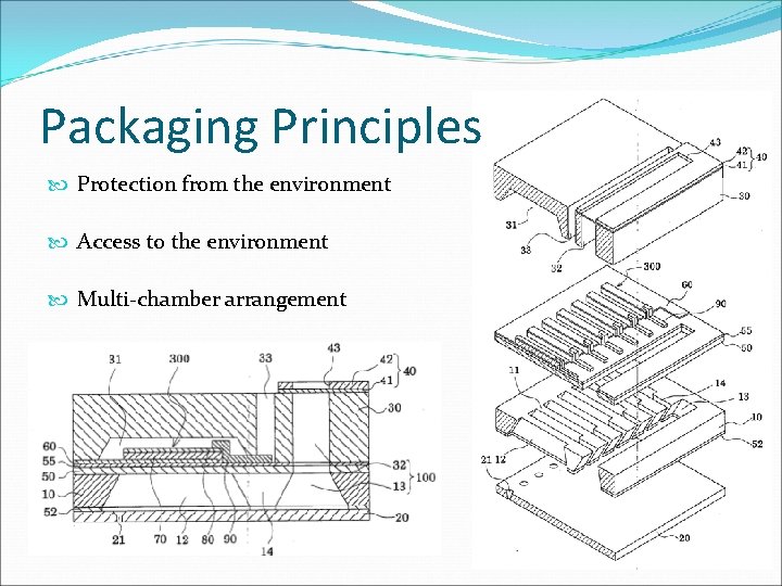
Packaging Principles Protection from the environment Access to the environment Multi-chamber arrangement
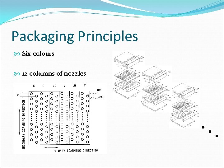
Packaging Principles Six colours 12 columns of nozzles
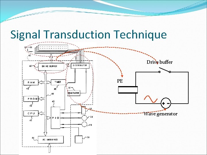
Signal Transduction Technique Drive buffer PE Wave generator
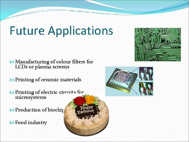
Future Applications Manufacturing of colour filters for LCDs or plasma screens Printing of ceramic materials Printing of electric circuits for microsystems Production of biochips Food industry
Questions?