Electronics for MEGII Donato Nicolo Pisa 15 January
- Slides: 23
Electronics for MEG-II Donato Nicolo` Pisa, 15 January 2014
Outlook • System overview – WD – DCB – Backplane – TCB • Status, agenda & milestones – Work in progress – Tests – Critical aspects delays? Electronics for MEG-II 2
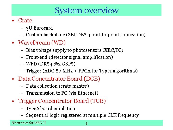
System overview • Crate – 3 U Eurocard – Custom backplane (SERDES point-to-point connection) • Wave. Dream (WD) – – Bias voltage supply to photosensors (XEC, TC) Front-end (detector signal amplification) WFD (DRS 4 @2 GSPS) Trigger (ADC 80 MHz + FPGA for Type 1 algorithms) • Data Concentrator Board (DCB) – Data collection (crate master) – Transmission to PC (via Ethernet) • Trigger Concentrator Board (TCB) – Type 2 board emulation – Sequential logic registered at multiple CLK frequency Electronics for MEG-II 3
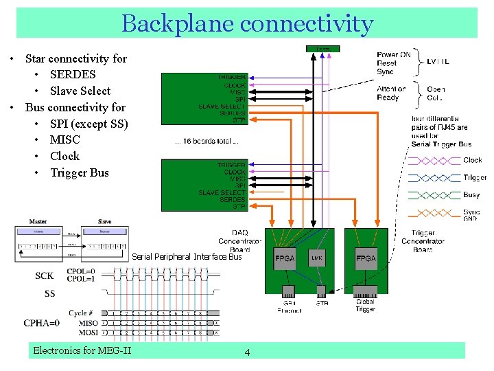
Backplane connectivity • Star connectivity for • SERDES • Slave Select • Bus connectivity for • SPI (except SS) • MISC • Clock • Trigger Bus Serial Peripheral Interface Bus Electronics for MEG-II 4
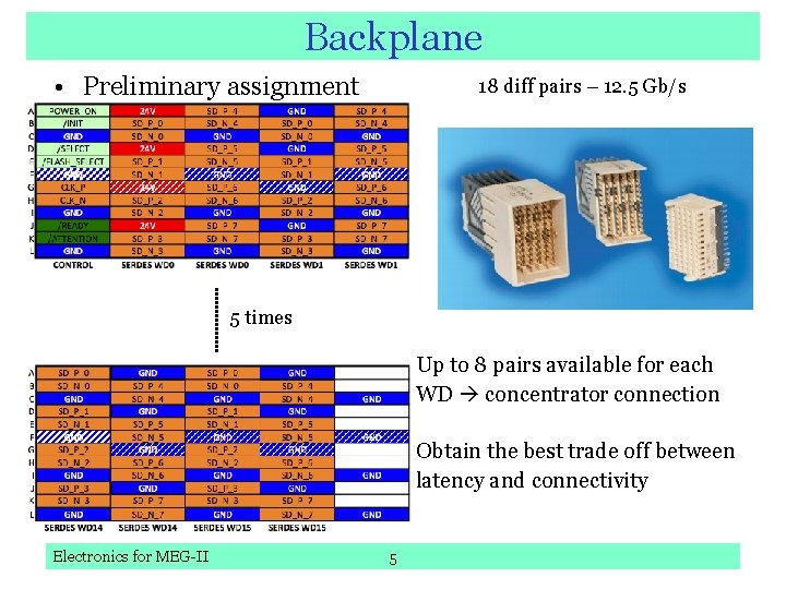
Backplane • Preliminary assignment 18 diff pairs – 12. 5 Gb/s 5 times Up to 8 pairs available for each WD concentrator connection Obtain the best trade off between latency and connectivity Electronics for MEG-II 5
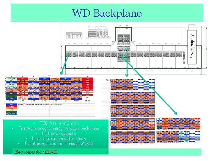
Power supply WD Backplane • • TCB fits in WD slot Firmware programming through backplane • Hot swap capable • High precision master clock • Fan & power control through MSCB Electronics for MEG-II 6
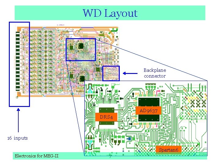
WD Layout Backplane connector AD 9637 DRS 4 16 inputs Spartan 6 Electronics for MEG-II 7
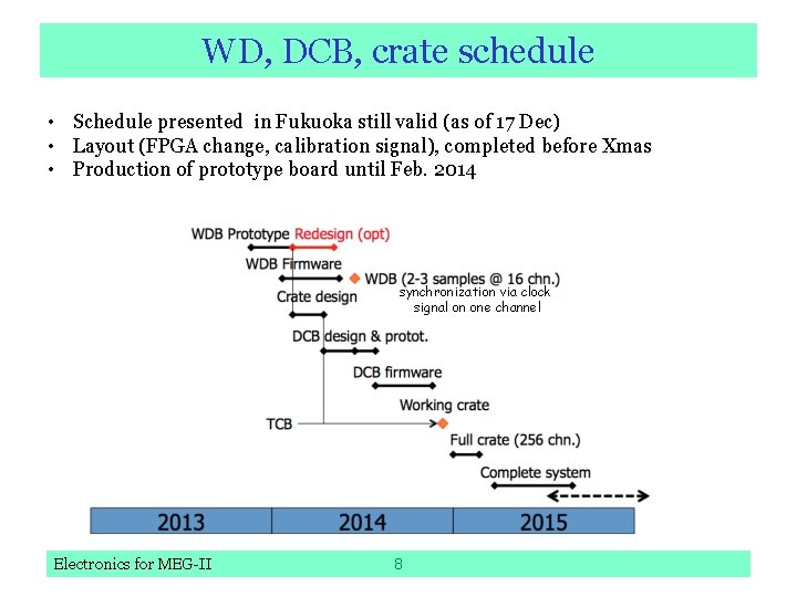
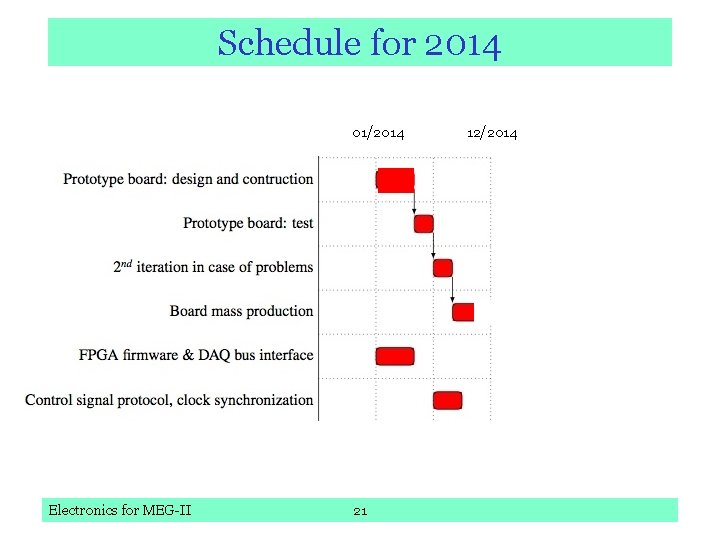
WD, DCB, crate schedule • Schedule presented in Fukuoka still valid (as of 17 Dec) • Layout (FPGA change, calibration signal), completed before Xmas • Production of prototype board until Feb. 2014 synchronization via clock signal on one channel Electronics for MEG-II 8
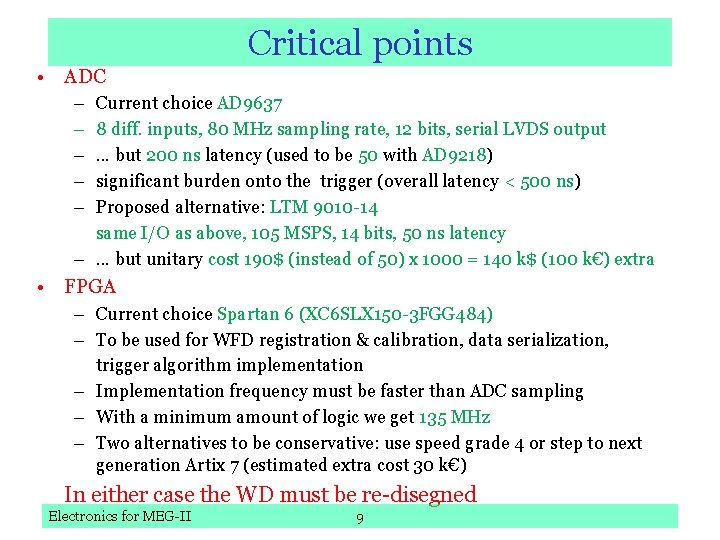
Critical points • ADC – – – Current choice AD 9637 8 diff. inputs, 80 MHz sampling rate, 12 bits, serial LVDS output. . . but 200 ns latency (used to be 50 with AD 9218) significant burden onto the trigger (overall latency < 500 ns) Proposed alternative: LTM 9010 -14 same I/O as above, 105 MSPS, 14 bits, 50 ns latency –. . . but unitary cost 190$ (instead of 50) x 1000 = 140 k$ (100 k€) extra • FPGA – Current choice Spartan 6 (XC 6 SLX 150 -3 FGG 484) – To be used for WFD registration & calibration, data serialization, trigger algorithm implementation – Implementation frequency must be faster than ADC sampling – With a minimum amount of logic we get 135 MHz – Two alternatives to be conservative: use speed grade 4 or step to next generation Artix 7 (estimated extra cost 30 k€) In either case the WD must be re-disegned Electronics for MEG-II 9
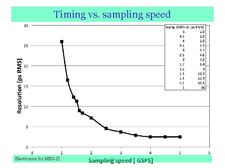
Timing vs. sampling speed Electronics for MEG-II 10
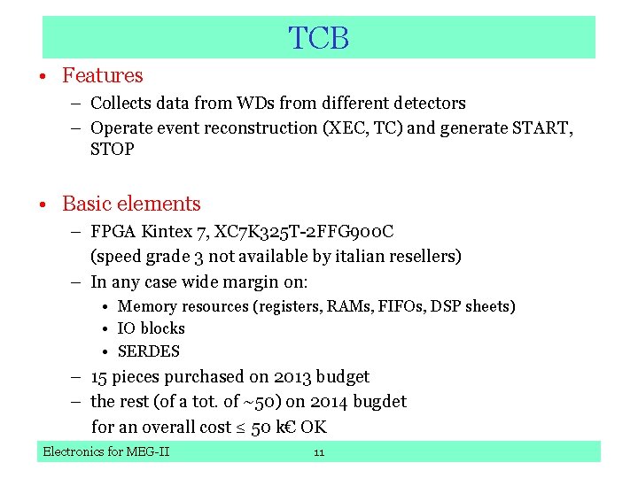
TCB • Features – Collects data from WDs from different detectors – Operate event reconstruction (XEC, TC) and generate START, STOP • Basic elements – FPGA Kintex 7, XC 7 K 325 T-2 FFG 900 C (speed grade 3 not available by italian resellers) – In any case wide margin on: • Memory resources (registers, RAMs, FIFOs, DSP sheets) • IO blocks • SERDES – 15 pieces purchased on 2013 budget – the rest (of a tot. of ~50) on 2014 bugdet for an overall cost ≤ 50 k€ OK Electronics for MEG-II 11
Critical issues and new features • Data bus handshaking – WD TCB • Expected throughput : 60 bit x 80 Mhz ~ 5 Gb/s from each WD Up to ~80 Gb/s data load on a low-level trigger concentrator (twice larger than current Master Type 2 board) with data serialization SERDES – TCB • Connections from/to different crates synchronous CLK needed, with the possibility to use different skews • L 2 trigger – algorithms • LUTs for hit lists track segments mapping to be implemented onto associative memories – options • Search on single board (track info to be transmitted to upper level board) • Track finder operated on master TCB • CLK synchronization • Backplane design and routing, master-slave protocol definition Electronics for MEG-II 12
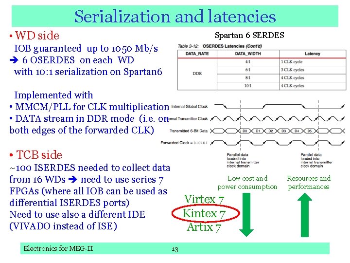
Serialization and latencies • WD side IOB guaranteed up to 1050 Mb/s 6 OSERDES on each WD with 10: 1 serialization on Spartan 6 SERDES Implemented with • MMCM/PLL for CLK multiplication • DATA stream in DDR mode (i. e. on both edges of the forwarded CLK) • TCB side ~100 ISERDES needed to collect data from 16 WDs need to use series 7 FPGAs (where all IOB can be used as differential ISERDES ports) Need to use also a different IDE (VIVADO instead of ISE) Electronics for MEG-II Low cost and power consumption Virtex 7 Kintex 7 Artix 7 13 Resources and performances
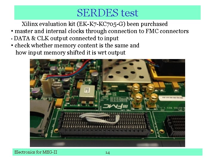
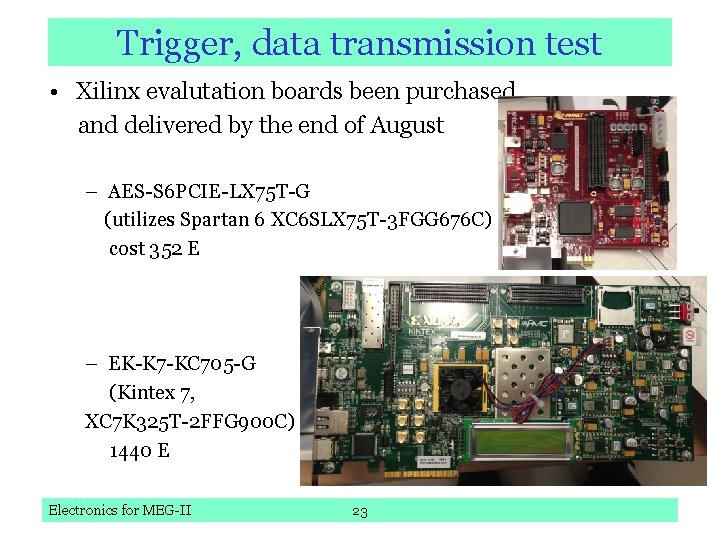
SERDES test Xilinx evaluation kit (EK-K 7 -KC 705 -G) been purchased • master and internal clocks through connection to FMC connectors • DATA & CLK output connected to input • check whether memory content is the same and how input memory shifted it is wrt output Electronics for MEG-II 14
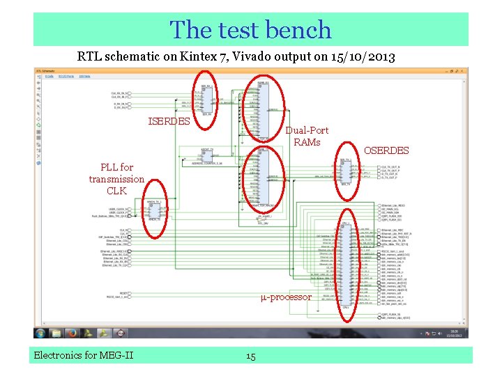
The test bench RTL schematic on Kintex 7, Vivado output on 15/10/2013 ISERDES Dual-Port RAMs PLL for transmission CLK -processor Electronics for MEG-II 15 OSERDES
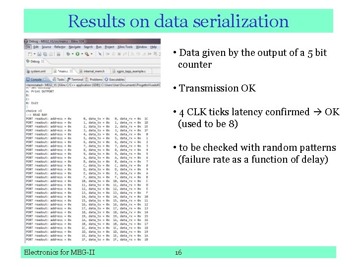
Results on data serialization • Data given by the output of a 5 bit counter • Transmission OK • 4 CLK ticks latency confirmed OK (used to be 8) • to be checked with random patterns (failure rate as a function of delay) Electronics for MEG-II 16
TCB link • Low level (~40 boards) – 60 output bits from any TCB, again 10: 1 serialization 6 data+1 CLK output 2 HDMI front D-type connectors • Intermediate level (~10 boards) – Fan-in 4: 1 8 HDMI D-type input connectors – Data output to master TCB through the backplane connector (the same as in the case of WD) direction inverted wrt low level boards – compatibility can be guaranteed • Top level (1 master board) – Located in the same crate as intermediate boards – Receives data and CLK from the backplane (the same way of low level boards) Electronics for MEG-II 17
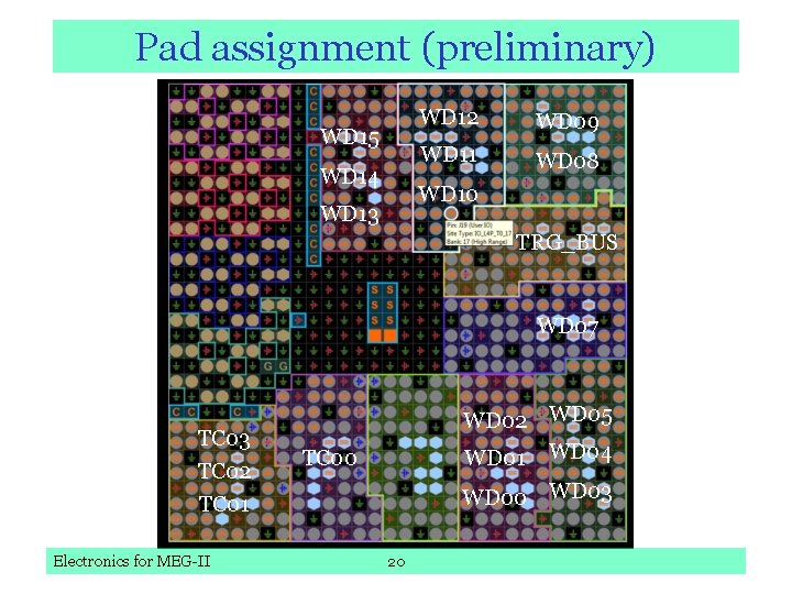
In progress • FPGA firmware development – I/O pad assignment – SERDES instantiation (input, output and possibly bidirectional) – algorithms • Board design – Connection to backplane and front panel – Conceptual layout – Routing to be started only after FW completion (due to constraints on CLK region) Electronics for MEG-II 18
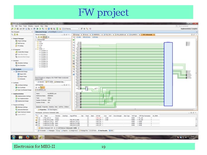
FW project Electronics for MEG-II 19
Pad assignment (preliminary) WD 15 WD 14 WD 12 WD 09 WD 11 WD 08 WD 10 WD 13 TRG_BUS WD 07 TC 03 TC 02 TC 01 Electronics for MEG-II TC 00 WD 02 WD 05 WD 01 WD 04 WD 00 WD 03 20
Schedule for 2014 01/2014 Electronics for MEG-II 21 12/2014
Conclusions • Electronics design going on • Board production in 2014 on time • Concerns about WD trigger capability in the current configuration • Other aspects to be checked as soon as prototypes are available • Backplane, DCB design supposed to go on in parallel • TCB – Serialization/deserialization protocol established – Firmware development going on – Board layout to follow timing constraint fit Electronics for MEG-II 22
Trigger, data transmission test • Xilinx evalutation boards been purchased and delivered by the end of August – AES-S 6 PCIE-LX 75 T-G (utilizes Spartan 6 XC 6 SLX 75 T-3 FGG 676 C) cost 352 E – EK-K 7 -KC 705 -G (Kintex 7, XC 7 K 325 T-2 FFG 900 C) 1440 E Electronics for MEG-II 23