EE 365 Readonly memories Static readwrite memories Dynamic
- Slides: 31

EE 365 Read-only memories Static read/write memories Dynamic read/write memories 1

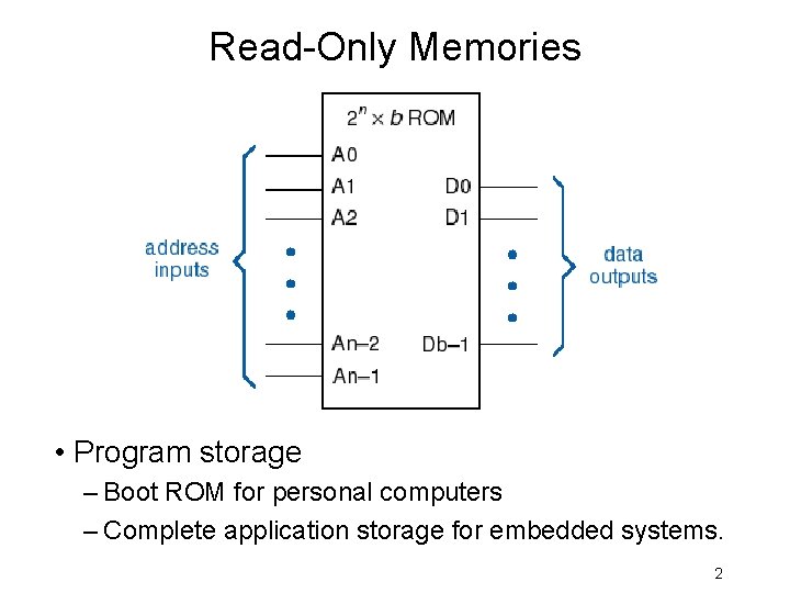
Read-Only Memories • Program storage – Boot ROM for personal computers – Complete application storage for embedded systems. 2

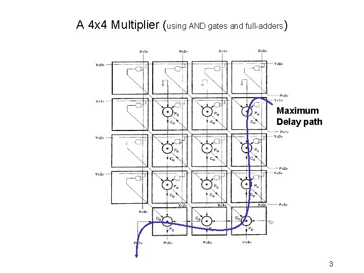
A 4 x 4 Multiplier (using AND gates and full-adders) Maximum Delay path 3

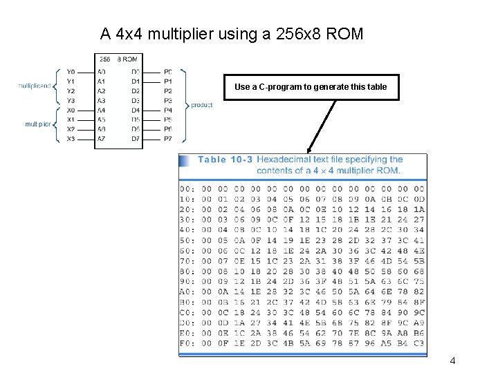
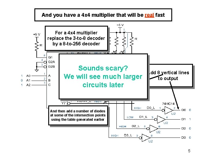
A 4 x 4 multiplier using a 256 x 8 ROM Use a C-program to generate this table 4

diagram of a 8 x 4 diode And. Logic you have a 4 x 4 multiplier that will be. ROM real fast For a 4 x 4 multiplier replace the 3 -to-8 decoder by a 8 -to-256 decoder Sounds scary? We will see much larger circuits later Add 8 vertical lines to output And then add a number of diodes at some of the intersection points using the table generated earlier 5

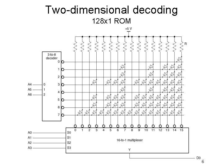
Two-dimensional decoding 128 x 1 ROM 6

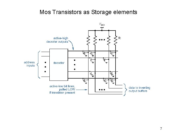
Mos Transistors as Storage elements 7

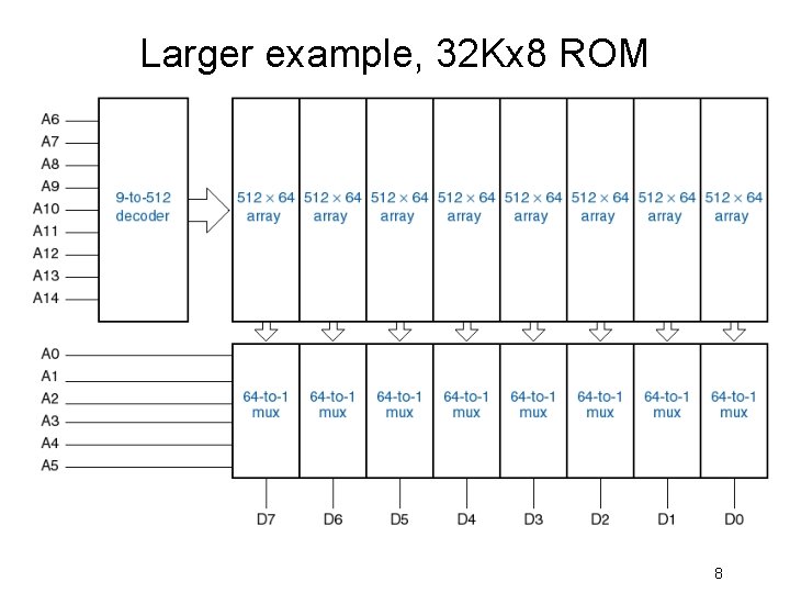
Larger example, 32 Kx 8 ROM 8

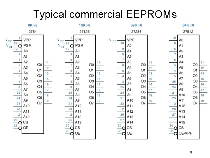
Typical commercial EEPROMs 9

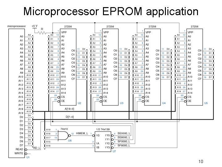
Microprocessor EPROM application 10

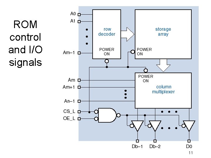
ROM control and I/O signals 11

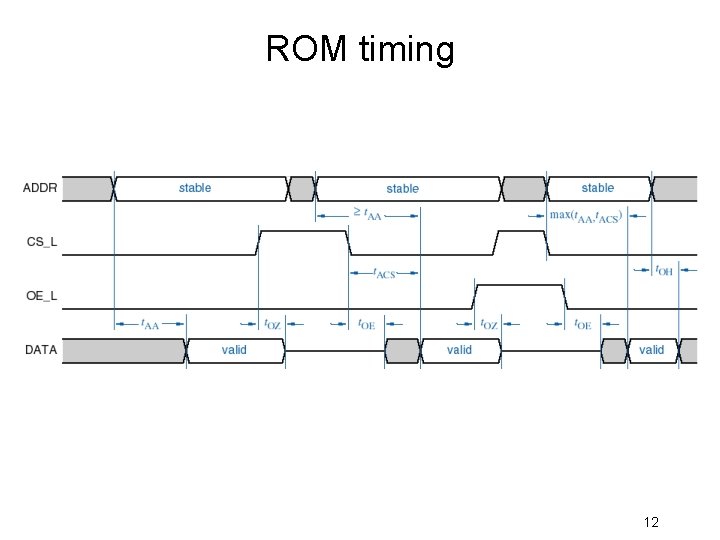
ROM timing 12

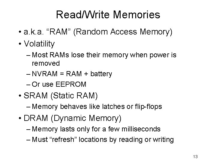
Read/Write Memories • a. k. a. “RAM” (Random Access Memory) • Volatility – Most RAMs lose their memory when power is removed – NVRAM = RAM + battery – Or use EEPROM • SRAM (Static RAM) – Memory behaves like latches or flip-flops • DRAM (Dynamic Memory) – Memory lasts only for a few milliseconds – Must “refresh” locations by reading or writing 13

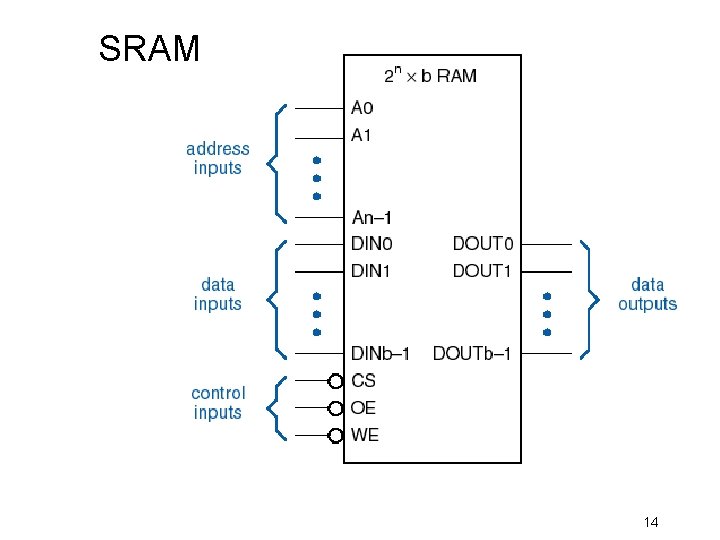
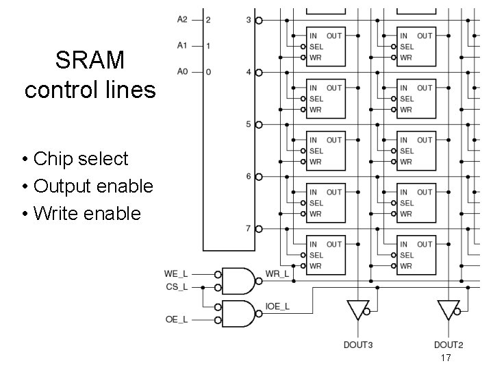
SRAM 14

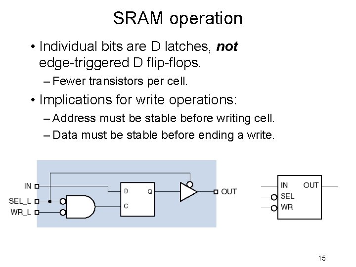
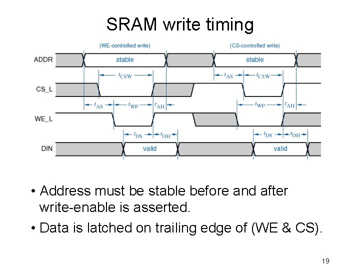
SRAM operation • Individual bits are D latches, not edge-triggered D flip-flops. – Fewer transistors per cell. • Implications for write operations: – Address must be stable before writing cell. – Data must be stable before ending a write. 15

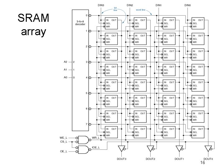
SRAM array 16

SRAM control lines • Chip select • Output enable • Write enable 17

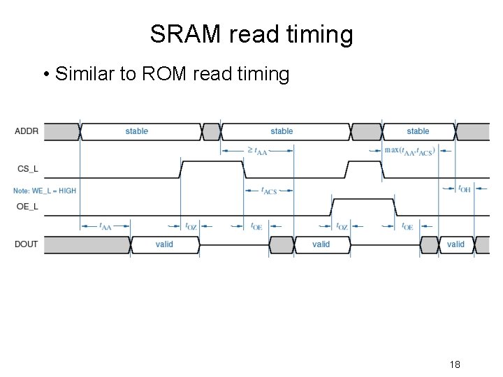
SRAM read timing • Similar to ROM read timing 18

SRAM write timing • Address must be stable before and after write-enable is asserted. • Data is latched on trailing edge of (WE & CS). 19

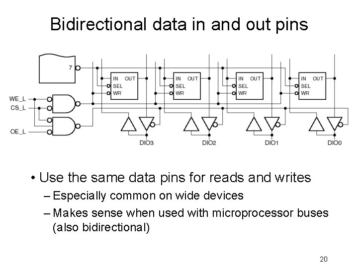
Bidirectional data in and out pins • Use the same data pins for reads and writes – Especially common on wide devices – Makes sense when used with microprocessor buses (also bidirectional) 20

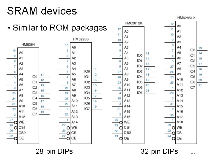
SRAM devices • Similar to ROM packages 28 -pin DIPs 32 -pin DIPs 21

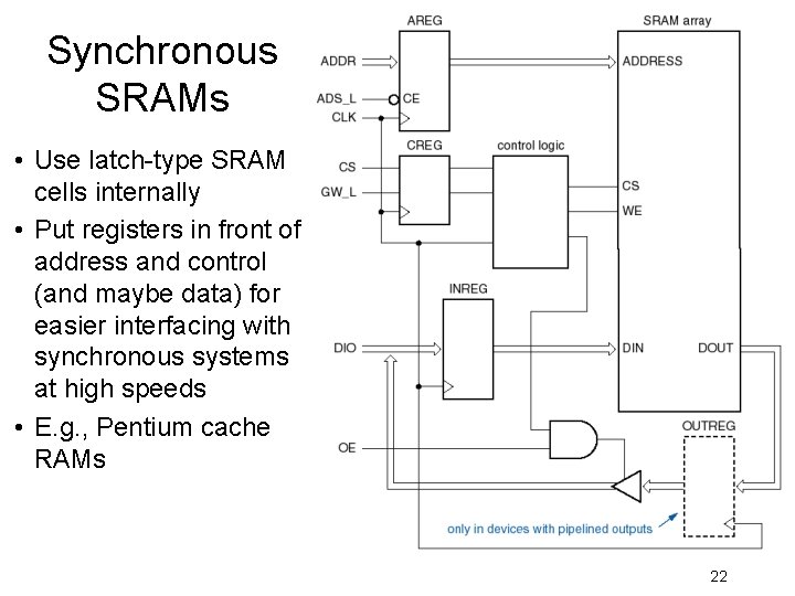
Synchronous SRAMs • Use latch-type SRAM cells internally • Put registers in front of address and control (and maybe data) for easier interfacing with synchronous systems at high speeds • E. g. , Pentium cache RAMs 22

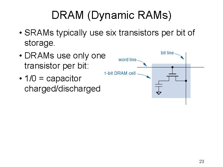
DRAM (Dynamic RAMs) • SRAMs typically use six transistors per bit of storage. • DRAMs use only one transistor per bit: • 1/0 = capacitor charged/discharged 23

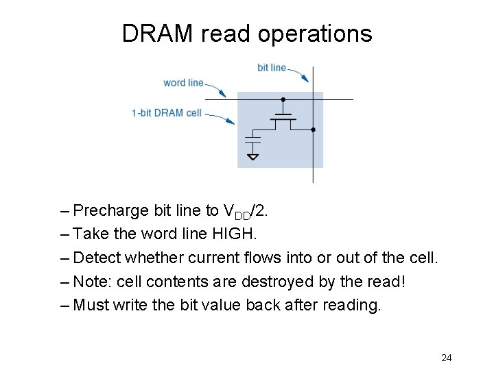
DRAM read operations – Precharge bit line to VDD/2. – Take the word line HIGH. – Detect whether current flows into or out of the cell. – Note: cell contents are destroyed by the read! – Must write the bit value back after reading. 24

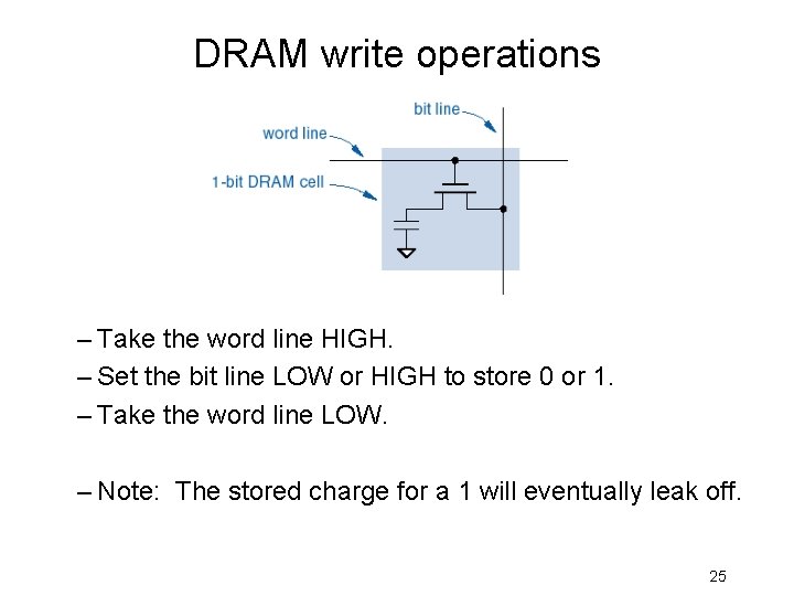
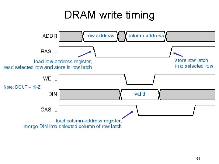
DRAM write operations – Take the word line HIGH. – Set the bit line LOW or HIGH to store 0 or 1. – Take the word line LOW. – Note: The stored charge for a 1 will eventually leak off. 25

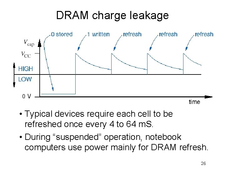
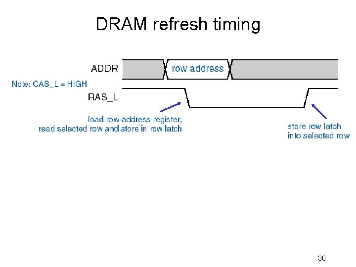
DRAM charge leakage • Typical devices require each cell to be refreshed once every 4 to 64 m. S. • During “suspended” operation, notebook computers use power mainly for DRAM refresh. 26

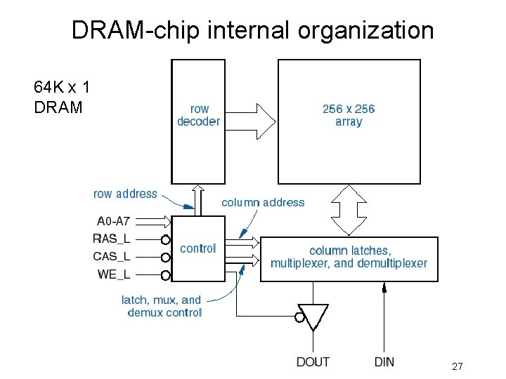
DRAM-chip internal organization 64 K x 1 DRAM 27

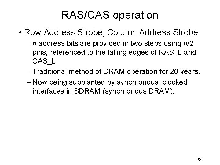
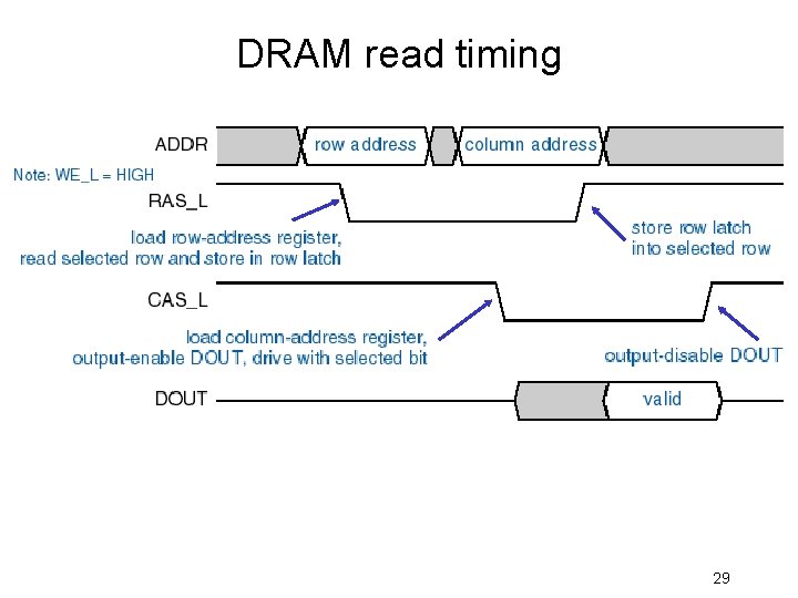
RAS/CAS operation • Row Address Strobe, Column Address Strobe – n address bits are provided in two steps using n/2 pins, referenced to the falling edges of RAS_L and CAS_L – Traditional method of DRAM operation for 20 years. – Now being supplanted by synchronous, clocked interfaces in SDRAM (synchronous DRAM). 28

DRAM read timing 29

DRAM refresh timing 30

DRAM write timing 31