Power Consumption in CMOS 1 Power Dissipation in


- Slides: 51

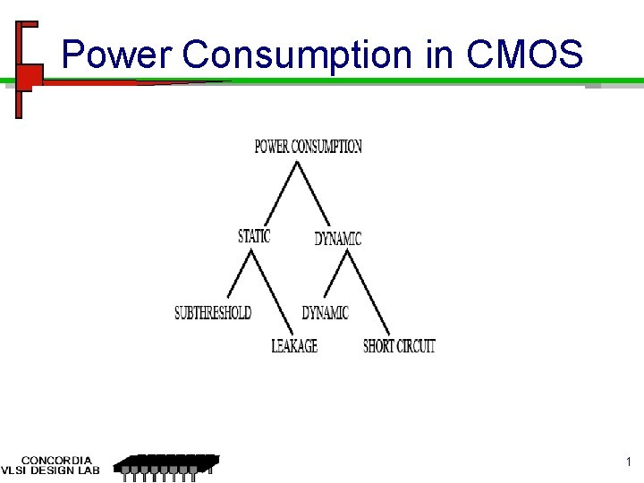
Power Consumption in CMOS 1

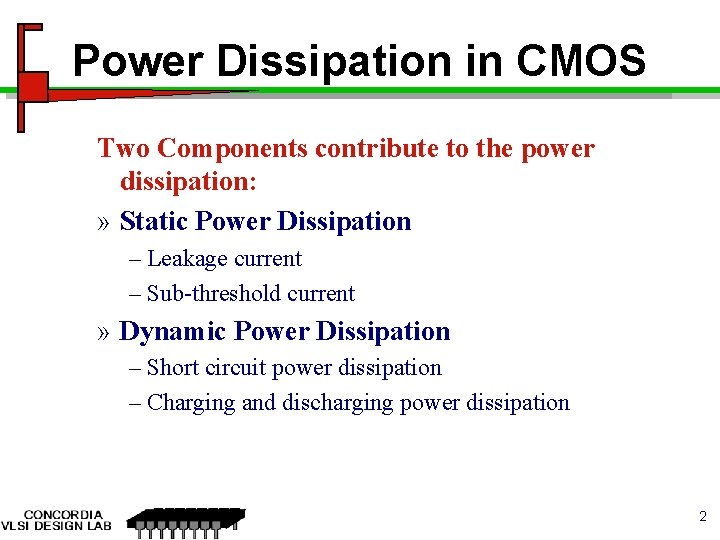
Power Dissipation in CMOS Two Components contribute to the power dissipation: » Static Power Dissipation – Leakage current – Sub-threshold current » Dynamic Power Dissipation – Short circuit power dissipation – Charging and discharging power dissipation 2

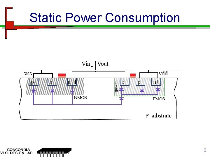
Static Power Consumption 3

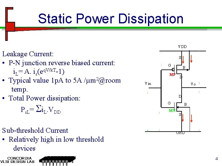
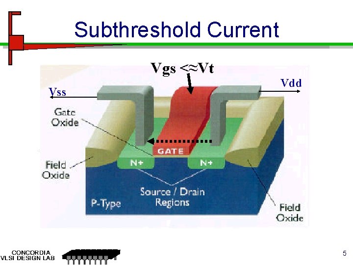
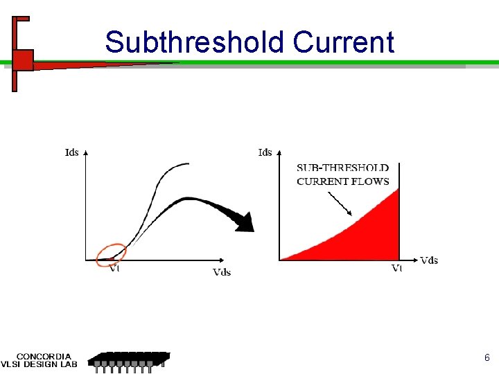
Static Power Dissipation VDD Leakage Current: • P-N junction reverse biased current: i. L= A. is(eq. V/k. T-1) • Typical value 1 p. A to 5 A /µm 2@room temp. • Total Power dissipation: Ps. L= i. L. VDD Sub-threshold Current • Relatively high in low threshold devices S G MP B D Vin Vo D G MN B S GND 4

Subthreshold Current Vgs <≈Vt Vss Vdd 5

Subthreshold Current 6

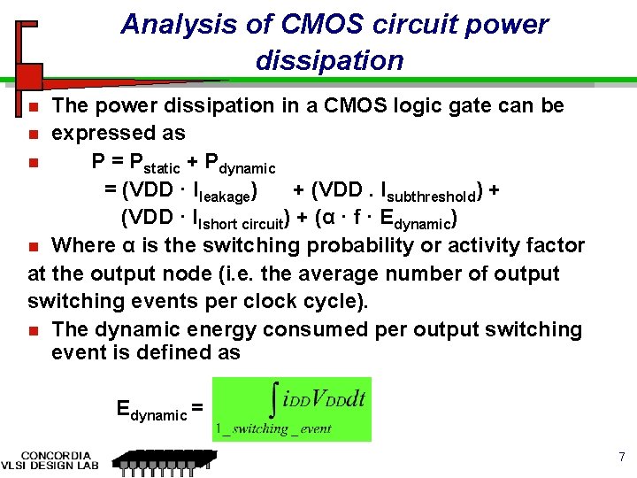
Analysis of CMOS circuit power dissipation The power dissipation in a CMOS logic gate can be n expressed as n P = Pstatic + Pdynamic = (VDD · Ileakage) + (VDD. Isubthreshold) + (VDD · Ilshort circuit) + (α · f · Edynamic) n Where α is the switching probability or activity factor at the output node (i. e. the average number of output switching events per clock cycle). n The dynamic energy consumed per output switching event is defined as n Edynamic = 7

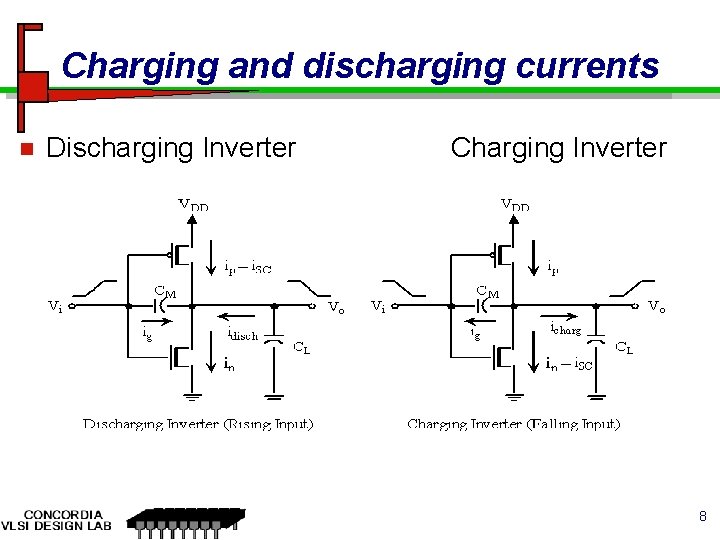
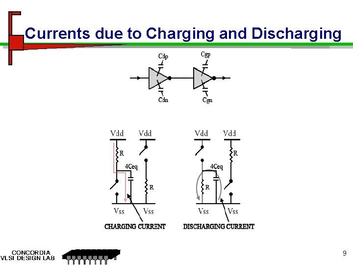
Charging and discharging currents n Discharging Inverter Charging Inverter 8

Currents due to Charging and Discharging 9

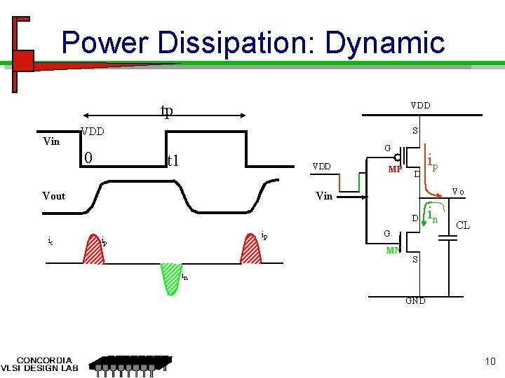
Power Dissipation: Dynamic VDD tp Vin VDD 0 S G t 1 VDD Vout MP D Vo Vin D ic ip ip ip G MN in CL S in GND 10

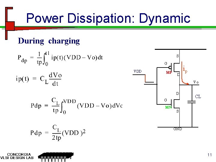
Power Dissipation: Dynamic During charging S G VDD MP D ip Vo D G MN CL S GND 11

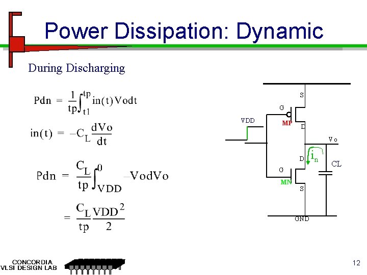
Power Dissipation: Dynamic During Discharging S G VDD MP D Vo D G MN in CL S GND 12

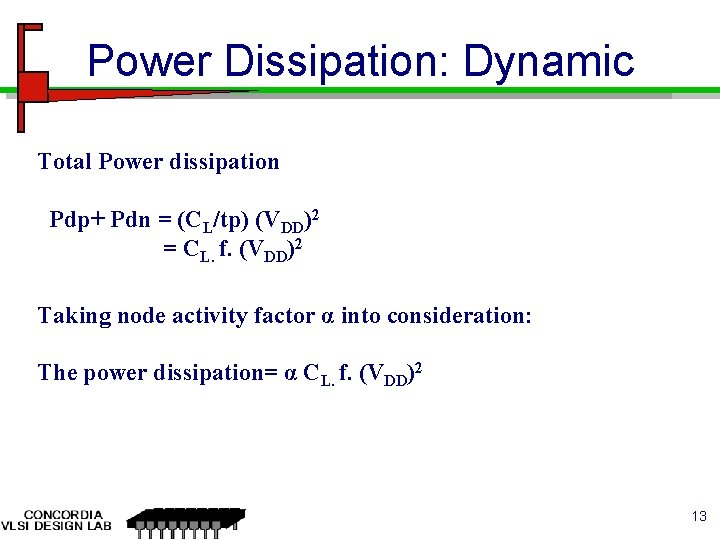
Power Dissipation: Dynamic Total Power dissipation Pdp+ Pdn = (CL/tp) (VDD)2 = CL. f. (VDD)2 Taking node activity factor α into consideration: The power dissipation= α CL. f. (VDD)2 13

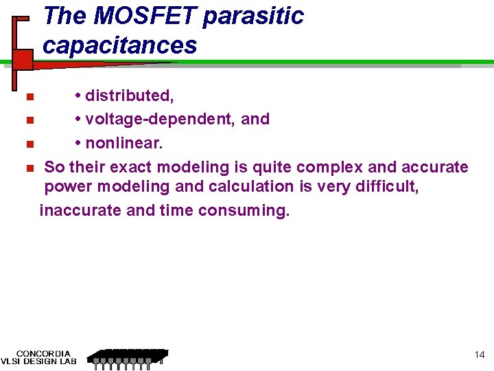
The MOSFET parasitic capacitances • distributed, n • voltage-dependent, and n • nonlinear. n So their exact modeling is quite complex and accurate power modeling and calculation is very difficult, inaccurate and time consuming. n 14

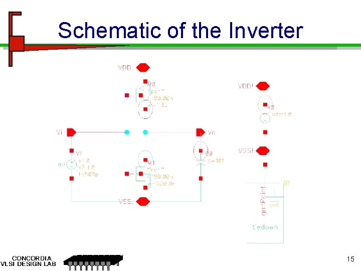
Schematic of the Inverter 15

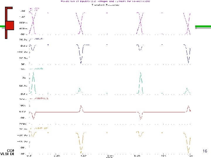
16

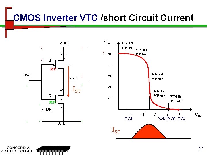
CMOS Inverter VTC /short Circuit Current V out VDD 5 S MN off MP lin MN sat MP lin 4 G D Vout D MN VGSN MN lin MP sat 1 G ISC MN sat MP sat 3 Vin 2 MP MN lin MP off S 1 VTN 2 3 4 5 VDD- |VTP| VDD V in GND ISC 17

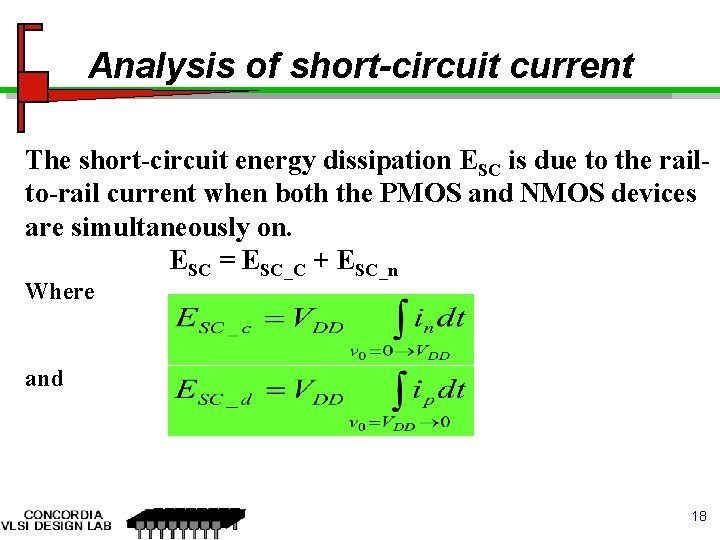
Analysis of short-circuit current The short-circuit energy dissipation ESC is due to the railto-rail current when both the PMOS and NMOS devices are simultaneously on. ESC = ESC_C + ESC_n Where and 18

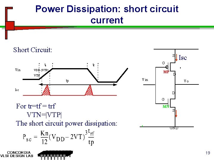
Power Dissipation: short circuit current Short Circuit: S tr Vin G tf VDD-|VTP| MP VTN tp Isc D Vin Vo Isc D G For tr=tf = trf VTN=|VTP| The short circuit power dissipation: MN S GND 19

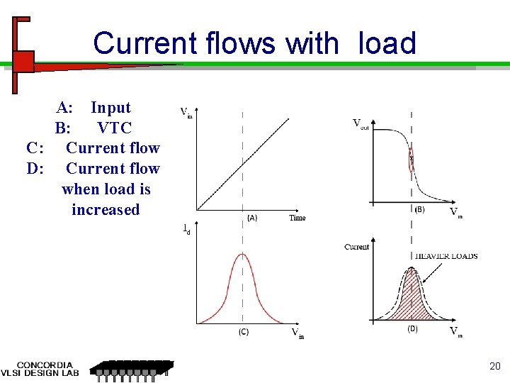
Current flows with load A: Input B: VTC C: Current flow D: Current flow when load is increased 20

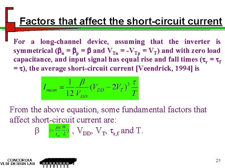
Factors that affect the short-circuit current For a long-channel device, assuming that the inverter is symmetrical ( n = p = and VTn = -VTp = VT) and with zero load capacitance, and input signal has equal rise and fall times ( r = f = ), the average short-circuit current [Veendrick, 1994] is From the above equation, some fundamental factors that affect short-circuit current are: , VDD, VT, r, f and T. 21

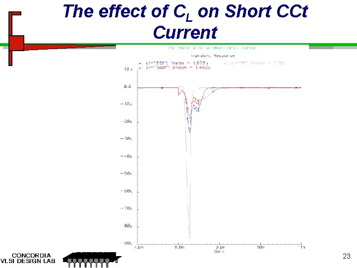
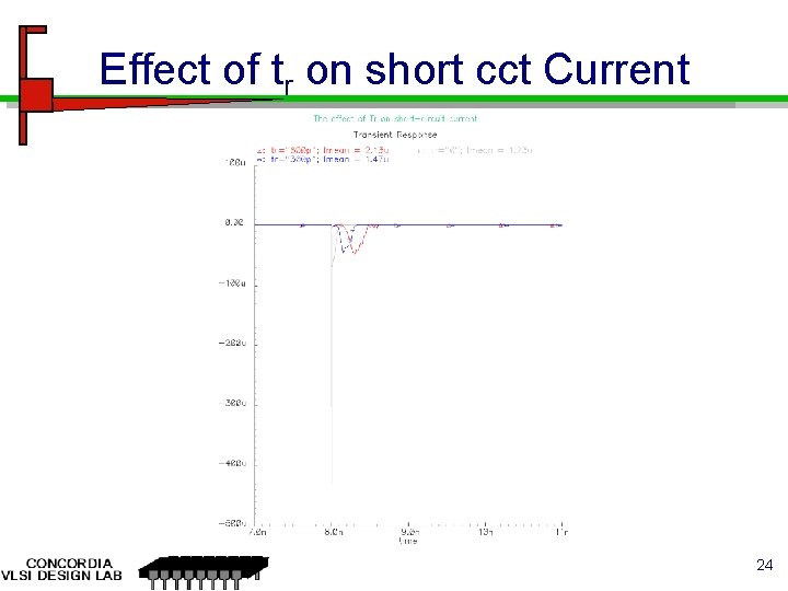
Parameters affecting short cct current For a short-channel device, and VT are no longer constants, but affected by a large number of parameters (i. e. circuit conditions, hspice parameters and process parameters). CL also affects short-circuit current. Imean is a function of the following parameters (tox is processdependent): CL, , T (or /T), VDD, Wn, p, Ln, p (or Wn, p/ Ln, p ), tox, … The above argument is validated by the means of simulation in the case of discharging inverter, 22

The effect of CL on Short CCt Current 23

Effect of tr on short cct Current 24

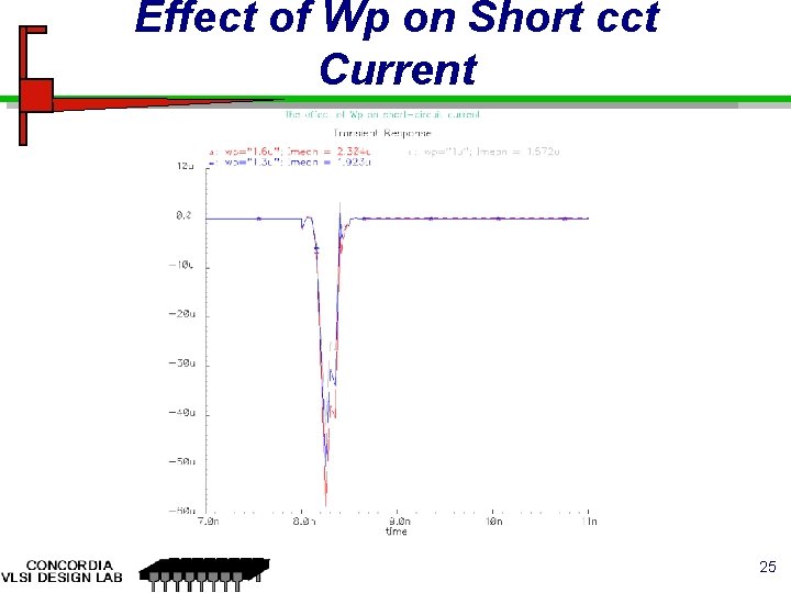
Effect of Wp on Short cct Current 25

Effect of time step setting on simulation results 26

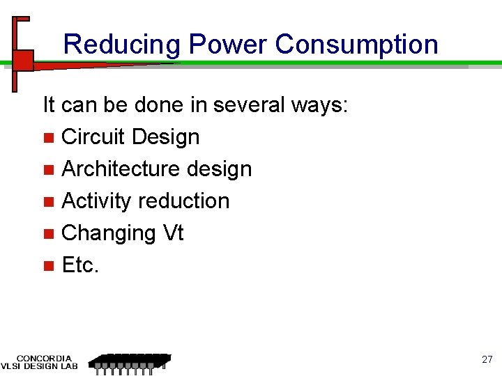
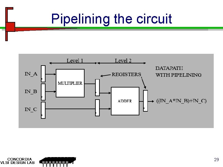
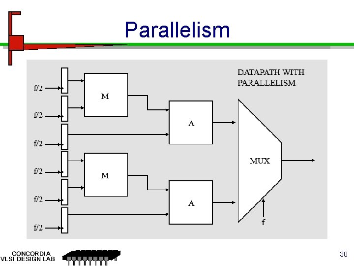
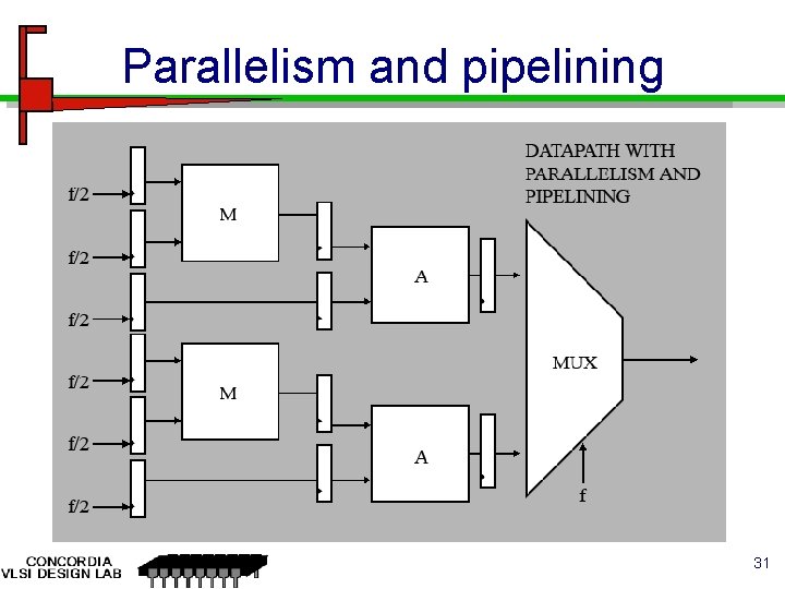
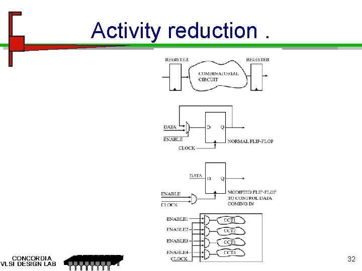
Reducing Power Consumption It can be done in several ways: n Circuit Design n Architecture design n Activity reduction n Changing Vt n Etc. 27

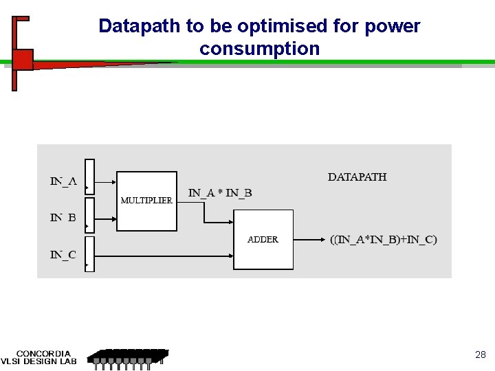
Datapath to be optimised for power consumption 28

Pipelining the circuit 29

Parallelism 30

Parallelism and pipelining 31

Activity reduction. 32

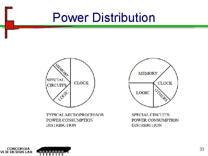
Power Distribution 33

Thank you ! 34

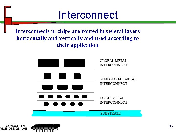
Interconnects in chips are routed in several layers horizontally and vertically and used according to their application 35

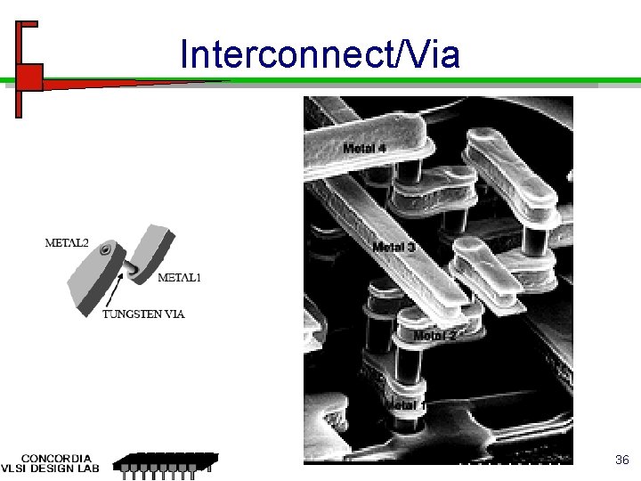
Interconnect/Via 36

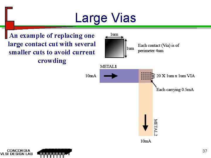
Large Vias An example of replacing one large contact cut with several smaller cuts to avoid current crowding 37

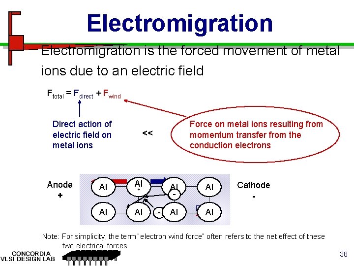
Electromigration is the forced movement of metal ions due to an electric field Ftotal = Fdirect + Fwind Direct action of electric field on metal ions Anode + Force on metal ions resulting from momentum transfer from the conduction electrons << Al Al Al + Al Al Al - Al Al E Cathode - Al- Note: For simplicity, the term “electron wind force” often refers to the net effect of these two electrical forces 38

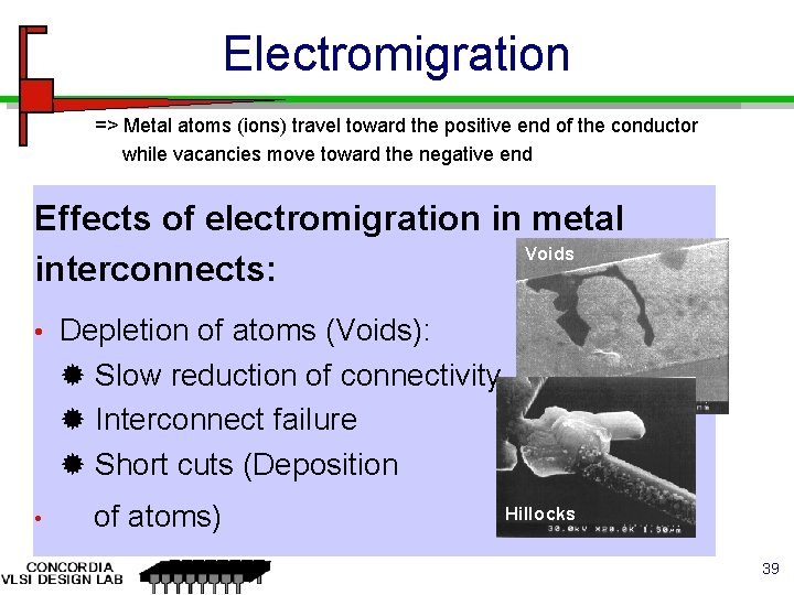
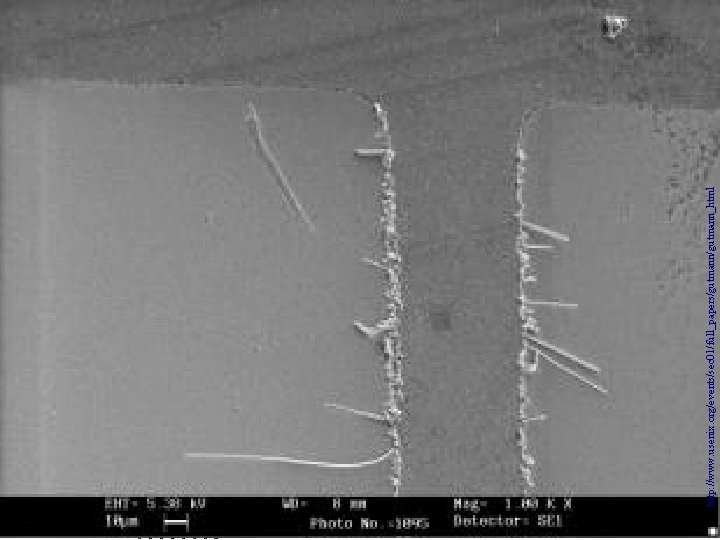
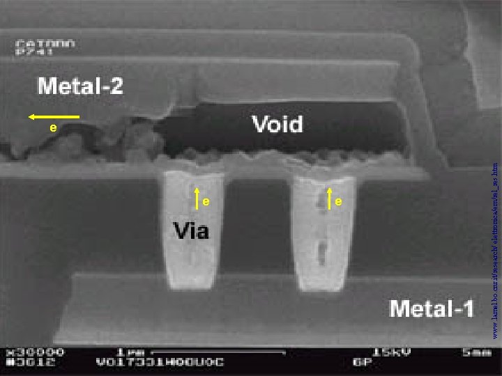
Electromigration => Metal atoms (ions) travel toward the positive end of the conductor while vacancies move toward the negative end Effects of electromigration in metal Voids interconnects: • Depletion of atoms (Voids): Slow reduction of connectivity Interconnect failure Short cuts (Deposition • of atoms) Hillocks 39

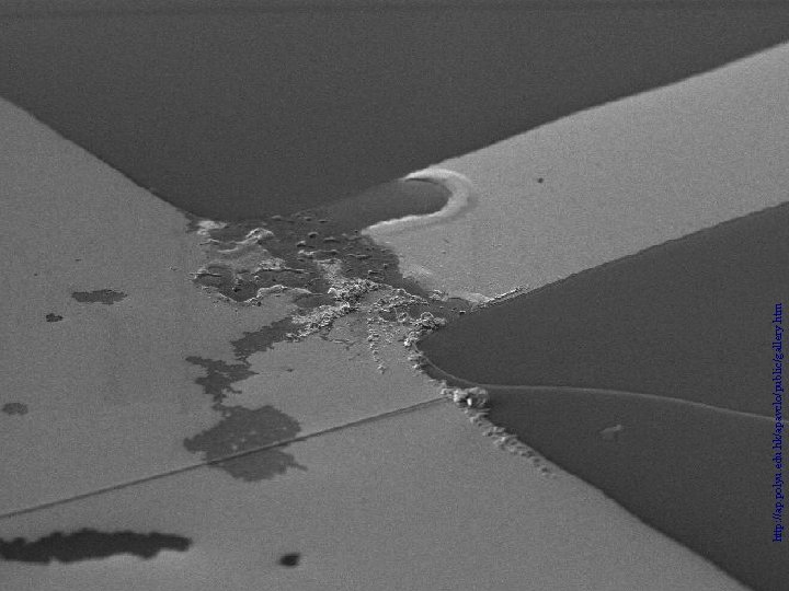
41 http: //ap. polyu. edu. hk/apavclo/public/gallery. htm

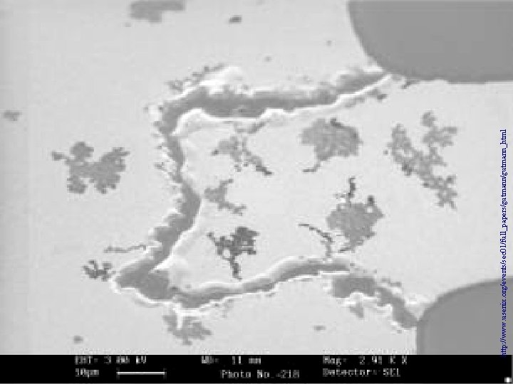
42 http: //www. usenix. org/events/sec 01/full_papers/gutmann_html

43 http: //www. usenix. org/events/sec 01/full_papers/gutmann_html

e e www. lamel. bo. cnr. it/research/ elettronica/em/rel_res. htm e 44

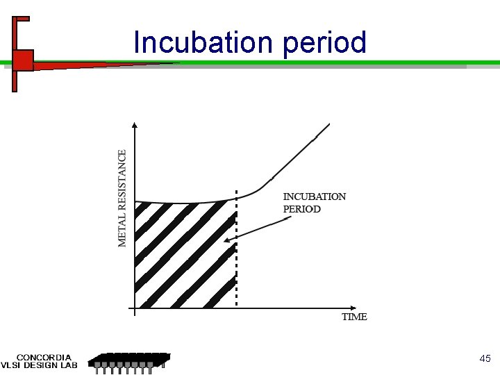
Incubation period 45

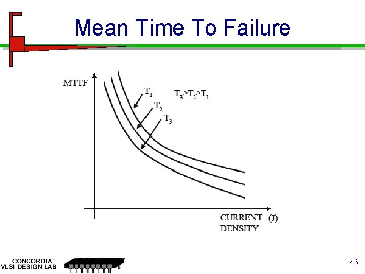
Mean Time To Failure 46

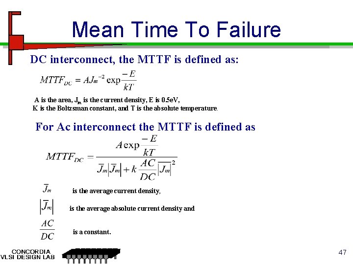
Mean Time To Failure DC interconnect, the MTTF is defined as: A is the area, Jm is the current density, E is 0. 5 e. V, K is the Boltzsman constant, and T is the absolute temperature. For Ac interconnect the MTTF is defined as is the average current density, is the average absolute current density and is a constant. 47

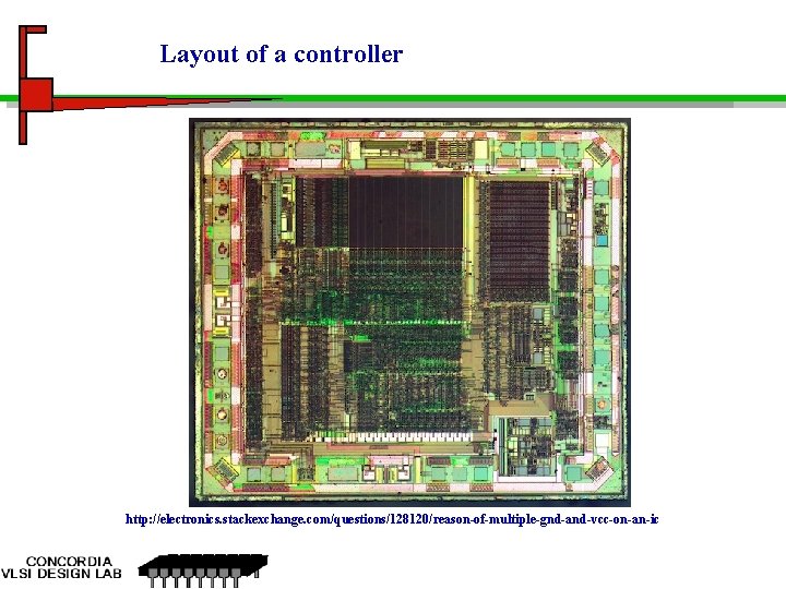
Layout of a controller http: //electronics. stackexchange. com/questions/128120/reason-of-multiple-gnd-and-vcc-on-an-ic

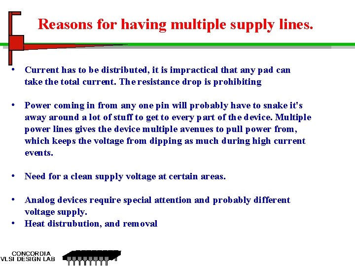
Reasons for having multiple supply lines. • Current has to be distributed, it is impractical that any pad can take the total current. The resistance drop is prohibiting • Power coming in from any one pin will probably have to snake it's away around a lot of stuff to get to every part of the device. Multiple power lines gives the device multiple avenues to pull power from, which keeps the voltage from dipping as much during high current events. • Need for a clean supply voltage at certain areas. • Analog devices require special attention and probably different voltage supply. • Heat distrubution, and removal

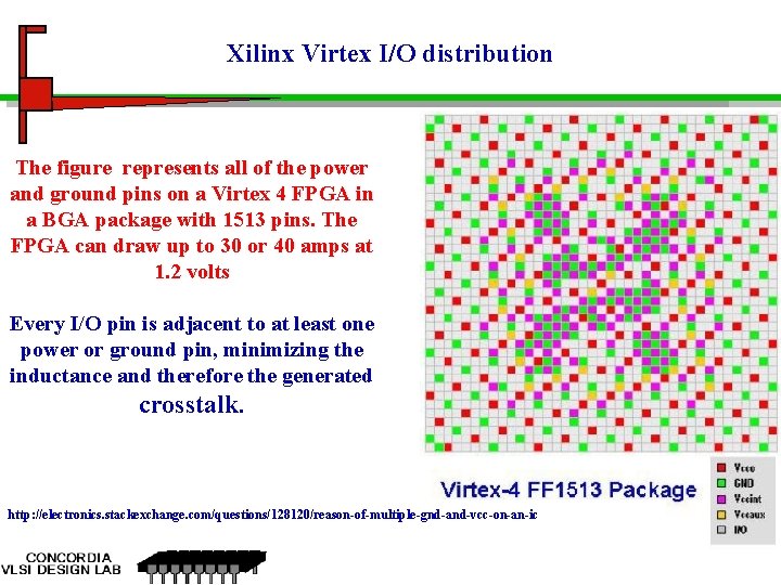
Xilinx Virtex I/O distribution The figure represents all of the power and ground pins on a Virtex 4 FPGA in a BGA package with 1513 pins. The FPGA can draw up to 30 or 40 amps at 1. 2 volts Every I/O pin is adjacent to at least one power or ground pin, minimizing the inductance and therefore the generated crosstalk. http: //electronics. stackexchange. com/questions/128120/reason-of-multiple-gnd-and-vcc-on-an-ic

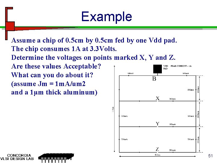
Example Assume a chip of 0. 5 cm by 0. 5 cm fed by one Vdd pad. The chip consumes 1 A at 3. 3 Volts. Determine the voltages on points marked X, Y and Z. Are these values Acceptable? What can you do about it? (assume Jm = 1 m. A/um 2 and a 1µm thick aluminum) 51

Thank you ! 52