Ecole Polytechnique Fdrale de Lausanne EPFL 3 D2


![3 D Experience in AQUA [2] – Confidential ● A. Carimatto, A. Ximenes, S. 3 D Experience in AQUA [2] – Confidential ● A. Carimatto, A. Ximenes, S.](https://slidetodoc.com/presentation_image_h2/ca0898eb05025f782a3b770e4631f507/image-13.jpg)

- Slides: 26

Ecole Polytechnique Fédérale de Lausanne EPFL 3 D/2. 5 D Integration, SPAD & System Specifications Francesco Gramuglia 1, Andrada Muntean 1, Myung-Jae Lee 1, Esteban Venialgo 2, Claudio Bruschini 1, Edoardo Charbon 1, 2 1 EPFL, Faculty of Microsystems and Microelectronics, Neuchâtel, Switzerland 2 Delft University of Technology, Faculty of Electrical Engineering, Circuits and Systems, Mekelweg 4, Delft, The Netherlands.

Outline ● Introduction ● Proposed Approaches ● Specifications & Current Research ● Conclusions 2

Outline ● Introduction ● Proposed Approaches ● Specifications & Current Research ● Conclusions 3

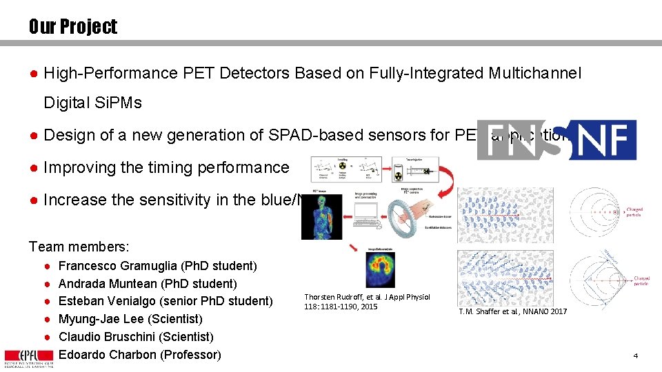
Our Project ● High-Performance PET Detectors Based on Fully-Integrated Multichannel Digital Si. PMs ● Design of a new generation of SPAD-based sensors for PET application ● Improving the timing performance ● Increase the sensitivity in the blue/NUV Team members: ● ● ● Francesco Gramuglia (Ph. D student) Andrada Muntean (Ph. D student) Esteban Venialgo (senior Ph. D student) Myung-Jae Lee (Scientist) Claudio Bruschini (Scientist) Edoardo Charbon (Professor) Thorsten Rudroff, et al. J Appl Physiol 118: 1181 -1190, 2015 T. M. Shaffer et al. , NNANO 2017 4

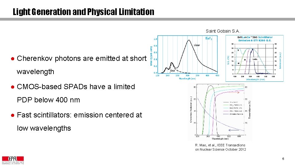
Light Generation and Physical Limitation Saint Gobain S. A. ● Cherenkov photons are emitted at short wavelength ● CMOS-based SPADs have a limited PDP below 400 nm ● Fast scintillators: emission centered at low wavelengths R. Mao, et al. , IEEE Transactions on Nuclear Science October 2012 5

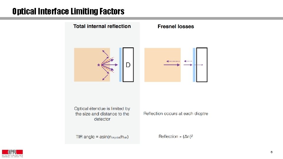
Optical Interface Limiting Factors 6

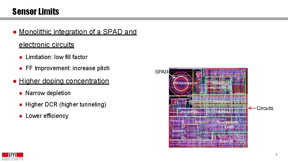
Sensor Limits ● Monolithic integration of a SPAD and electronic circuits ● Limitation: low fill factor ● FF Improvement: increase pitch ● Higher doping concentration ● Narrow depletion ● Higher DCR (higher tunneling) ● Lower efficiency 7

Outline ● Introduction ● Proposed Approaches ● Specifications & Current Research ● Conclusions 8

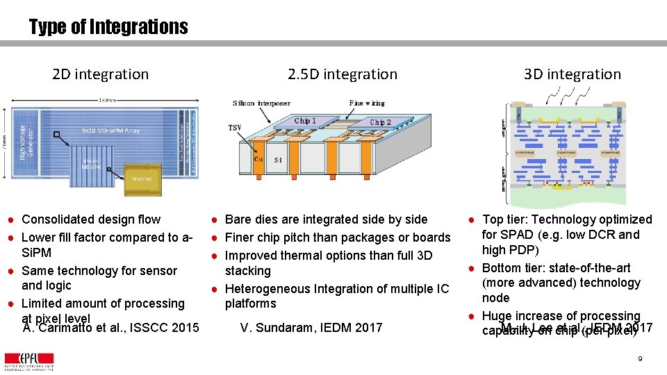
Type of Integrations 2 D integration ● Consolidated design flow ● Lower fill factor compared to a. Si. PM ● Same technology for sensor and logic ● Limited amount of processing at pixel level A. Carimatto et al. , ISSCC 2015 2. 5 D integration ● Bare dies are integrated side by side ● Finer chip pitch than packages or boards ● Improved thermal options than full 3 D stacking ● Heterogeneous Integration of multiple IC platforms V. Sundaram, IEDM 2017 3 D integration ● Top tier: Technology optimized for SPAD (e. g. low DCR and high PDP) ● Bottom tier: state-of-the-art (more advanced) technology node ● Huge increase of processing M. -J. Lee et al. , (per IEDM 2017 capability on chip pixel) 9

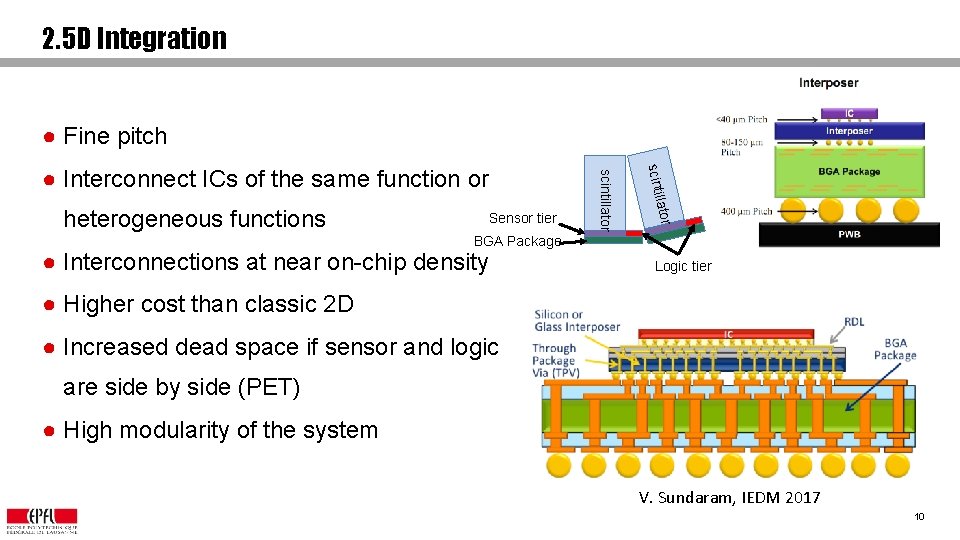
2. 5 D Integration ● Fine pitch llator Sensor tier scinti heterogeneous functions scintillator ● Interconnect ICs of the same function or BGA Package ● Interconnections at near on-chip density Logic tier ● Higher cost than classic 2 D ● Increased dead space if sensor and logic are side by side (PET) ● High modularity of the system V. Sundaram, IEDM 2017 10

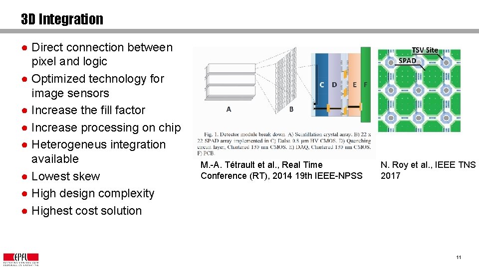
3 D Integration ● Direct connection between pixel and logic ● Optimized technology for image sensors ● Increase the fill factor ● Increase processing on chip ● Heterogeneus integration available ● Lowest skew ● High design complexity ● Highest cost solution M. -A. Tétrault et al. , Real Time Conference (RT), 2014 19 th IEEE-NPSS N. Roy et al. , IEEE TNS 2017 11

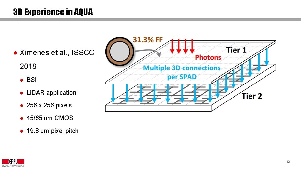
3 D Experience in AQUA ● Ximenes et al. , ISSCC 2018 ● BSI ● Li. DAR application ● 256 x 256 pixels ● 45/65 nm CMOS ● 19. 8 um pixel pitch 13
![3 D Experience in AQUA 2 Confidential A Carimatto A Ximenes S 3 D Experience in AQUA [2] – Confidential ● A. Carimatto, A. Ximenes, S.](https://slidetodoc.com/presentation_image_h2/ca0898eb05025f782a3b770e4631f507/image-13.jpg)
3 D Experience in AQUA [2] – Confidential ● A. Carimatto, A. Ximenes, S. 65 nm top tier Lidner. Intended for ISSCC 40 nm bottom Conf. registers tier Quadrant electronics 2019 L C ● BSI Quadrant electronics TDC ● Li. DAR application Quadrant electronics digital core Quadrant electronics adders/regs IO adders/regs ● Two halves: 32 x 64 and 64 x 128 SPADs ● 19. 8 um and 9. 4 um pixel ● 78% and 35% Fill Factor 1 pixel comprises 1 pitch SPAD 1 pixel comprises 4 SPADs g digital memory ● 40/65 nm CMOS electronics per quenchin pixel Timing line ● Digital read-out 14

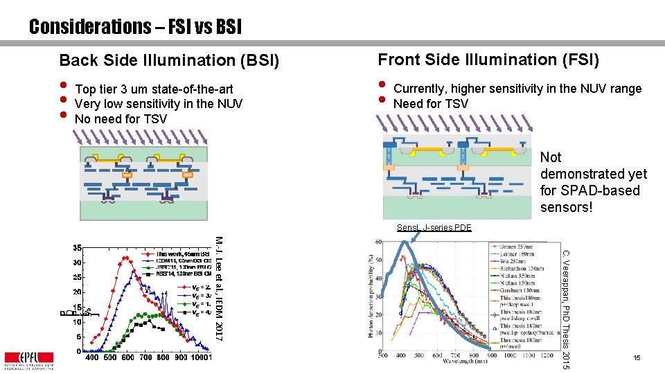
Considerations – FSI vs BSI Back Side Illumination (BSI) Front Side Illumination (FSI) • Top tier 3 um state-of-the-art • Very low sensitivity in the NUV • No need for TSV • Currently, higher sensitivity in the NUV range • Need for TSV Not demonstrated yet for SPAD-based sensors! Sens. L J-series PDE C. Veerappan, Ph. D Thesis 2015 M. -J. Lee et al. , IEDM 2017 15

Outline ● Introduction ● Proposed Approaches ● Current Research & Specifications ● Conclusions 17

Our Targets & Current research ● New NUV optimized SPAD structures under development ● Design of a new optimized TDC architecture ● Study the 2. 5 D/3 D integration 18

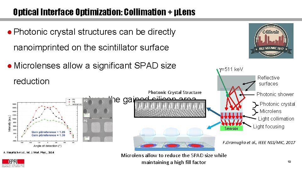
Optical Interface Optimization: Collimation + μLens ● Photonic crystal structures can be directly nanoimprinted on the scintillator surface ● Microlenses allow a significant SPAD size g=511 ke. V Reflective surfaces reduction Photonic Crystal Structure Photonic shower ● Several ways to (re)use the gained silicon area Photonic crystal Microlens Light collimation Sensor Light focusing F. Gramuglia et al. , IEEE NSS/MIC, 2017 A. Knapitsch et al. , Int. J. Mod. Phys. , 2014 Microlens allow to reduce the SPAD size while maintaining a high fill factor 19

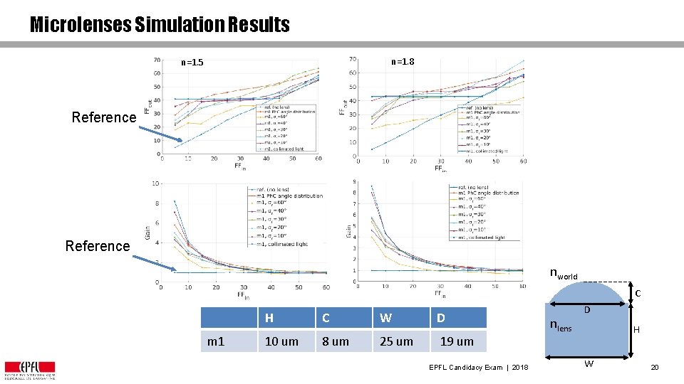
Microlenses Simulation Results n=1. 8 n=1. 5 Reference nworld C m 1 H C W D 10 um 8 um 25 um 19 um EPFL Candidacy Exam | 2018 nlens D H W 20

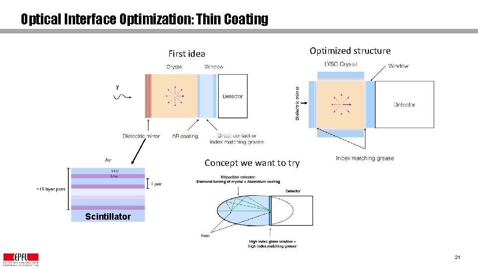
Optical Interface Optimization: Thin Coating Optimized structure Dielectric mirror First idea Concept we want to try Scintillator 21

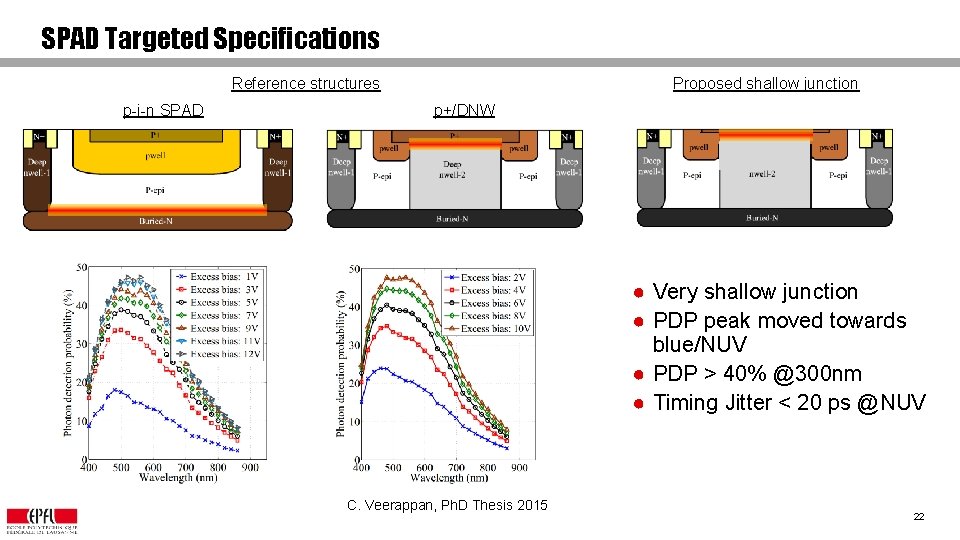
SPAD Targeted Specifications Proposed shallow junction Reference structures p-i-n SPAD p+/DNW ● Very shallow junction ● PDP peak moved towards blue/NUV ● PDP > 40% @300 nm ● Timing Jitter < 20 ps @NUV C. Veerappan, Ph. D Thesis 2015 22

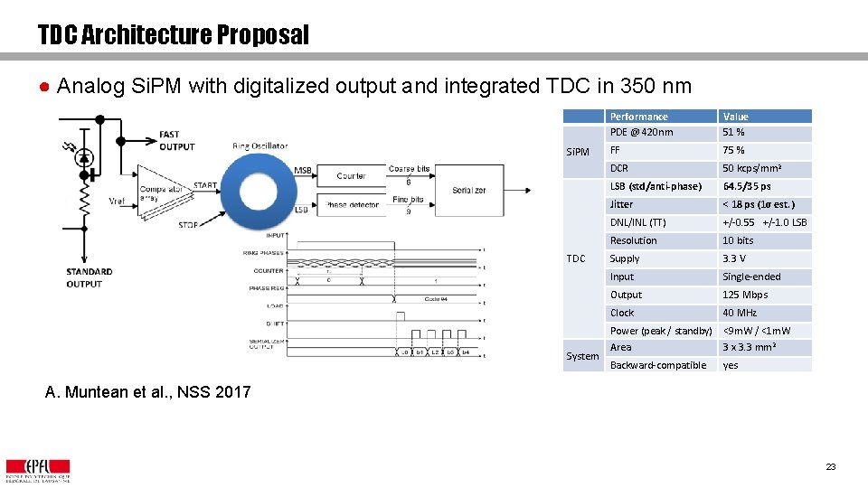
TDC Architecture Proposal ● Analog Si. PM with digitalized output and integrated TDC in 350 nm Si. PM TDC System Performance PDE @ 420 nm Value 51 % FF 75 % DCR 50 kcps/mm 2 LSB (std/anti-phase) 64. 5/35 ps Jitter < 18 ps (1σ est. ) DNL/INL (TT) +/-0. 55 +/-1. 0 LSB Resolution 10 bits Supply 3. 3 V Input Single-ended Output 125 Mbps Clock 40 MHz Power (peak / standby) <9 m. W / <1 m. W Area 3 x 3. 3 mm 2 Backward-compatible yes A. Muntean et al. , NSS 2017 23

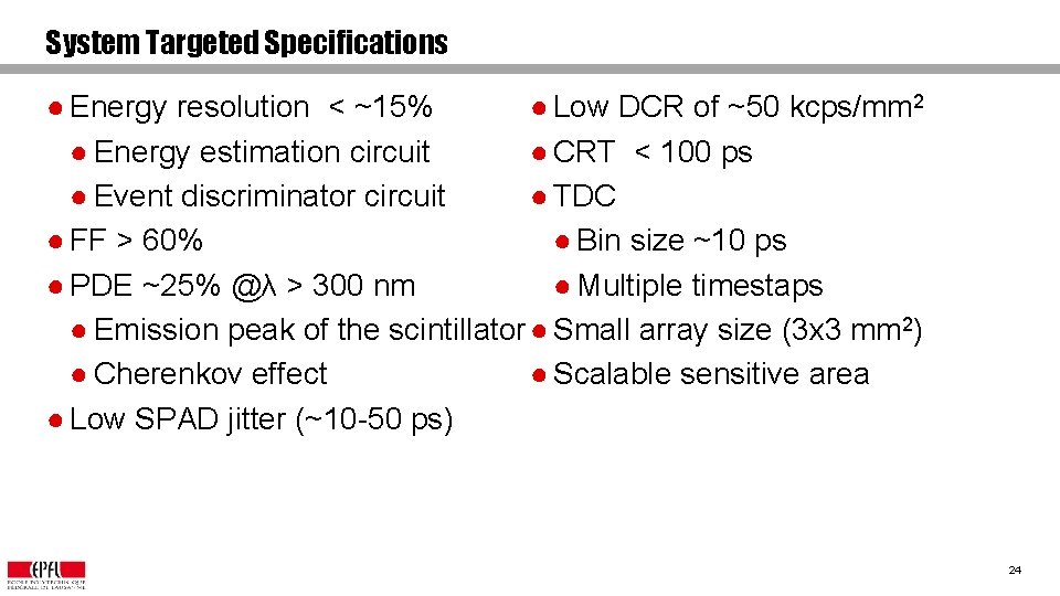
System Targeted Specifications ● Low DCR of ~50 kcps/mm 2 ● Energy resolution < ~15% ● CRT < 100 ps ● Energy estimation circuit ● TDC ● Event discriminator circuit ● Bin size ~10 ps ● FF > 60% ● Multiple timestaps ● PDE ~25% @λ > 300 nm ● Emission peak of the scintillator ● Small array size (3 x 3 mm 2) ● Scalable sensitive area ● Cherenkov effect ● Low SPAD jitter (~10 -50 ps) 24

Outline ● Introduction ● Proposed Approaches ● Specifications & Current Research ● Conclusions 25

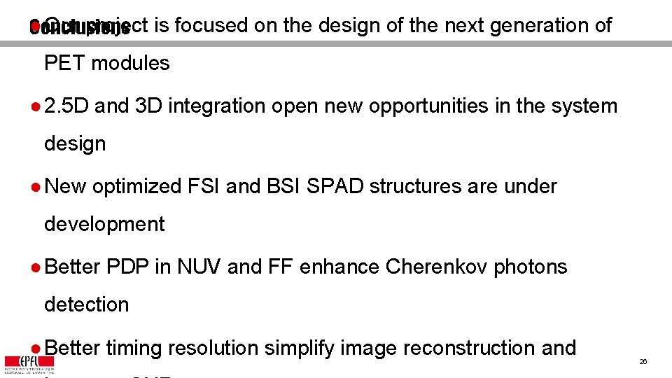
● Our project is focused on the design of the next generation of Conclusions PET modules ● 2. 5 D and 3 D integration open new opportunities in the system design ● New optimized FSI and BSI SPAD structures are under development ● Better PDP in NUV and FF enhance Cherenkov photons detection ● Better timing resolution simplify image reconstruction and 26

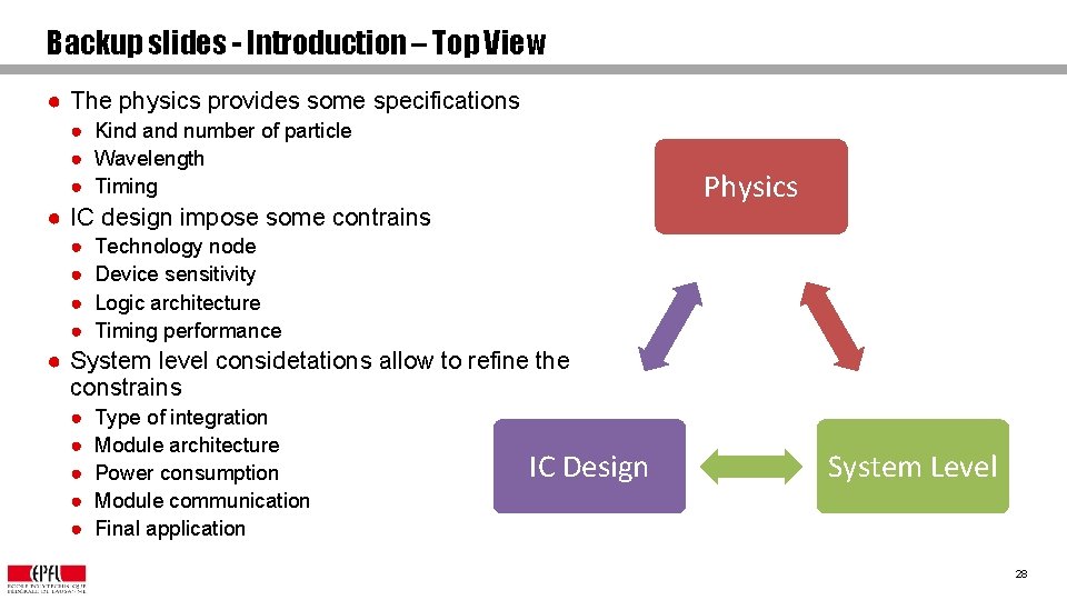
Backup slides - Introduction – Top View ● The physics provides some specifications ● Kind and number of particle ● Wavelength ● Timing Physics ● IC design impose some contrains ● ● Technology node Device sensitivity Logic architecture Timing performance ● System level considetations allow to refine the constrains ● ● ● Type of integration Module architecture Power consumption Module communication Final application IC Design System Level 28

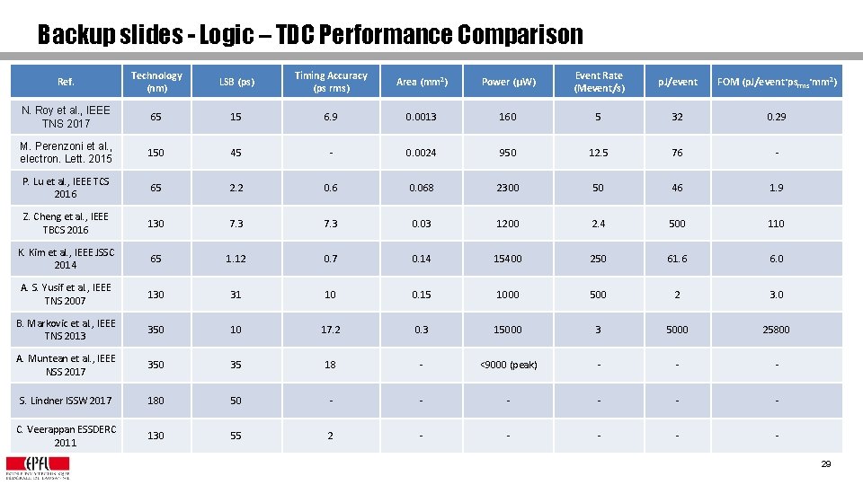
Backup slides - Logic – TDC Performance Comparison Ref. Technology (nm) LSB (ps) Timing Accuracy (ps rms) Area (mm 2) Power (μW) Event Rate (Mevent/s) p. J/event FOM (p. J/event·psrms·mm 2) N. Roy et al. , IEEE TNS 2017 65 15 6. 9 0. 0013 160 5 32 0. 29 M. Perenzoni et al. , electron. Lett. 2015 150 45 - 0. 0024 950 12. 5 76 - P. Lu et al. , IEEE TCS 2016 65 2. 2 0. 6 0. 068 2300 50 46 1. 9 Z. Cheng et al. , IEEE TBCS 2016 130 7. 3 0. 03 1200 2. 4 500 110 K. Kim et al. , IEEE JSSC 2014 65 1. 12 0. 7 0. 14 15400 250 61. 6 6. 0 A. S. Yusif et al. , IEEE TNS 2007 130 31 10 0. 15 1000 500 2 3. 0 B. Markovic et al. , IEEE TNS 2013 350 10 17. 2 0. 3 15000 3 5000 25800 A. Muntean et al. , IEEE NSS 2017 350 35 18 - <9000 (peak) - - - S. Lindner ISSW 2017 180 50 - - - C. Veerappan ESSDERC 2011 130 55 2 - - 29