ECE 875 Electronic Devices Prof Virginia Ayres Electrical
- Slides: 28

ECE 875: Electronic Devices Prof. Virginia Ayres Electrical & Computer Engineering Michigan State University ayresv@msu. edu

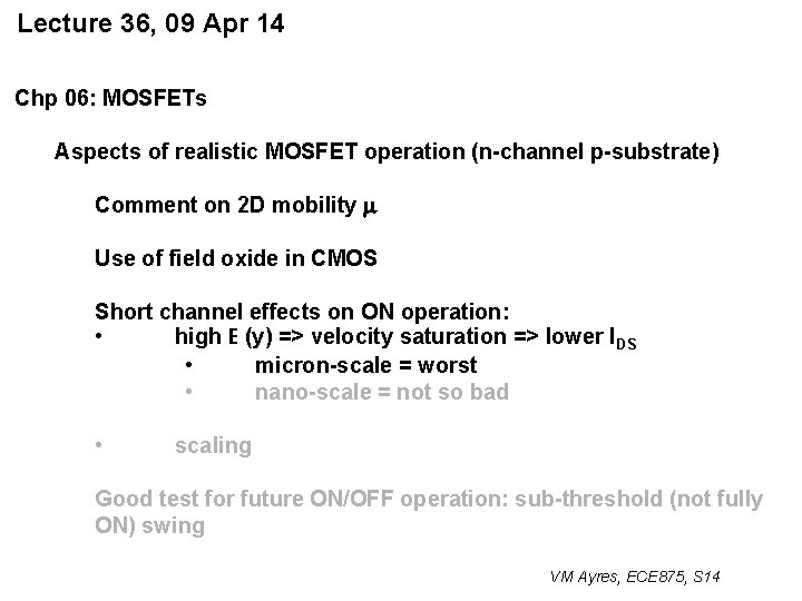
Lecture 36, 09 Apr 14 Chp 06: MOSFETs Aspects of realistic MOSFET operation (n-channel p-substrate) Comment on 2 D mobility m Use of field oxide in CMOS Short channel effects on ON operation: • high E (y) => velocity saturation => lower IDS • micron-scale = worst • nano-scale = not so bad • scaling Good test for future ON/OFF operation: sub-threshold (not fully ON) swing VM Ayres, ECE 875, S 14

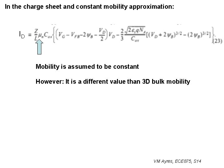
In the charge sheet and constant mobility approximation: ID Mobility is assumed to be constant However: It is a different value than 3 D bulk mobility VM Ayres, ECE 875, S 14

Lecture 36, 09 Apr 14 Chp 06: MOSFETs Aspects of realistic MOSFET operation (n-channel p-substrate) Comment on 2 D mobility m Use of field oxide in CMOS Short channel effects on ON operation: • high E (y) => velocity saturation => lower IDS • micron-scale = worst • nano-scale = not so bad • scaling Good test for future ON/OFF operation: sub-threshold (not fully ON) swing VM Ayres, ECE 875, S 14

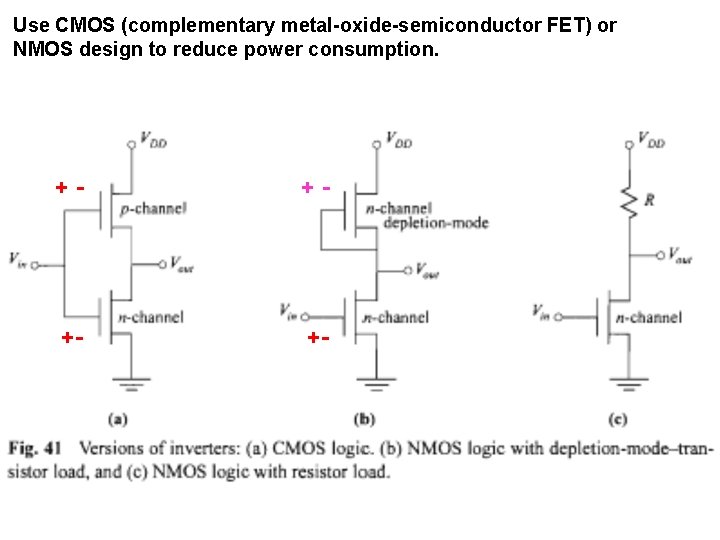
Use CMOS (complementary metal-oxide-semiconductor FET) or NMOS design to reduce power consumption. +- +-

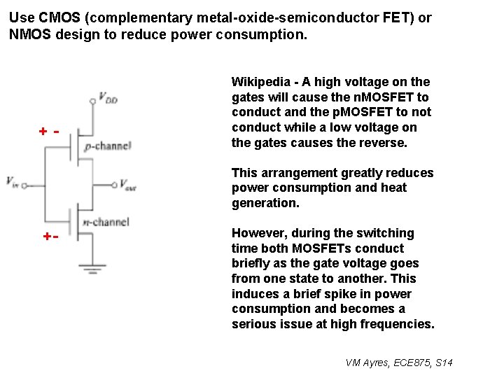
Use CMOS (complementary metal-oxide-semiconductor FET) or NMOS design to reduce power consumption. +- Wikipedia - A high voltage on the gates will cause the n. MOSFET to conduct and the p. MOSFET to not conduct while a low voltage on the gates causes the reverse. This arrangement greatly reduces power consumption and heat generation. +- However, during the switching time both MOSFETs conduct briefly as the gate voltage goes from one state to another. This induces a brief spike in power consumption and becomes a serious issue at high frequencies. VM Ayres, ECE 875, S 14

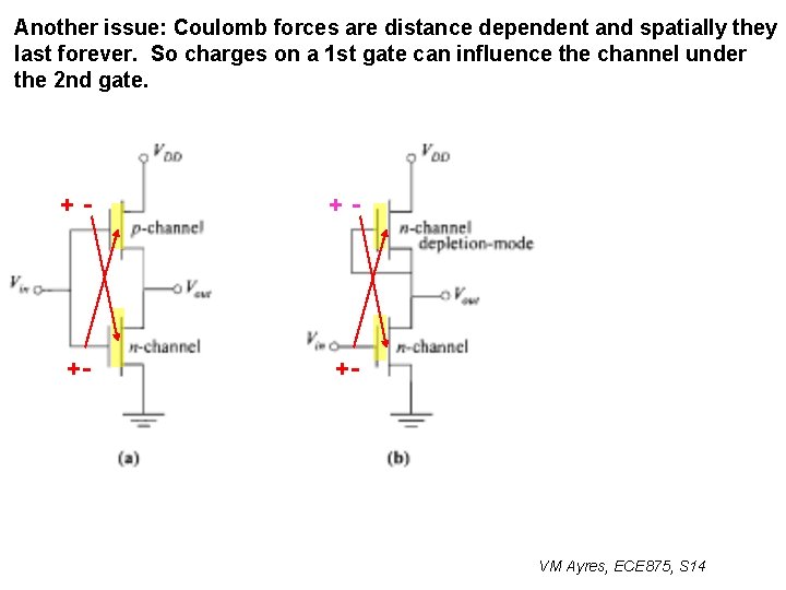
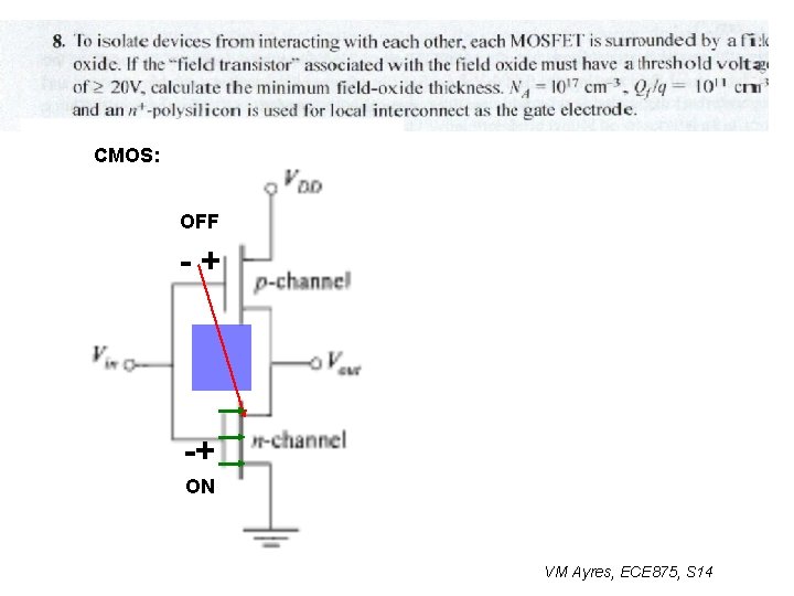
Another issue: Coulomb forces are distance dependent and spatially they last forever. So charges on a 1 st gate can influence the channel under the 2 nd gate. +- +- VM Ayres, ECE 875, S 14

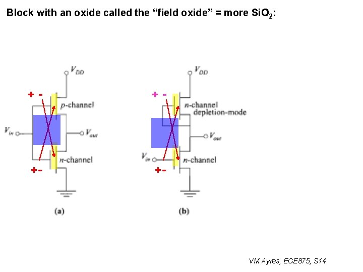
Block with an oxide called the “field oxide” = more Si. O 2: +- +- VM Ayres, ECE 875, S 14

CMOS: OFF -+ -+ ON VM Ayres, ECE 875, S 14

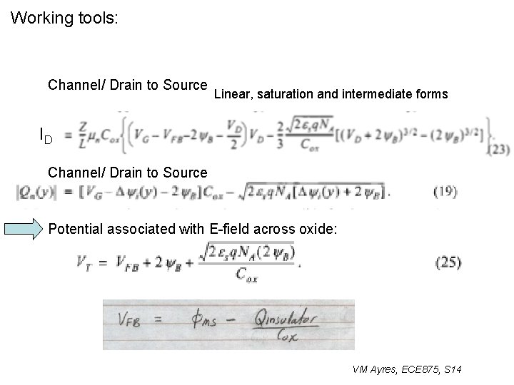
Working tools: Channel/ Drain to Source Linear, saturation and intermediate forms ID Channel/ Drain to Source Potential associated with E-field across oxide: VM Ayres, ECE 875, S 14

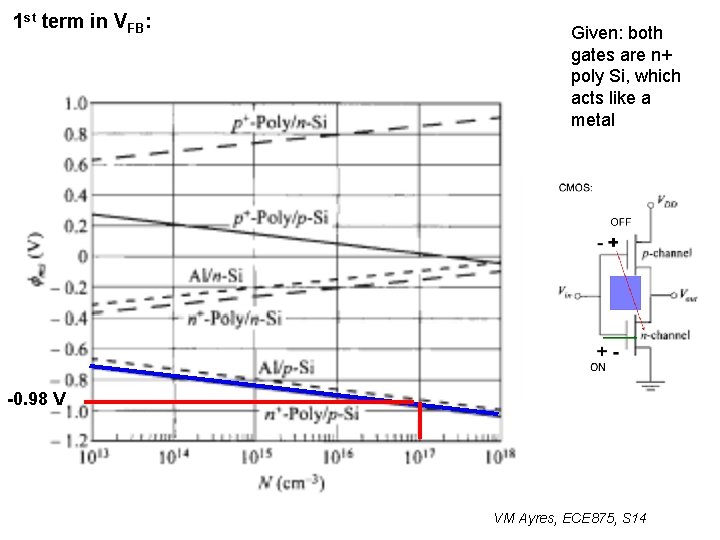
1 st term in VFB: Given: both gates are n+ poly Si, which acts like a metal -0. 98 V VM Ayres, ECE 875, S 14

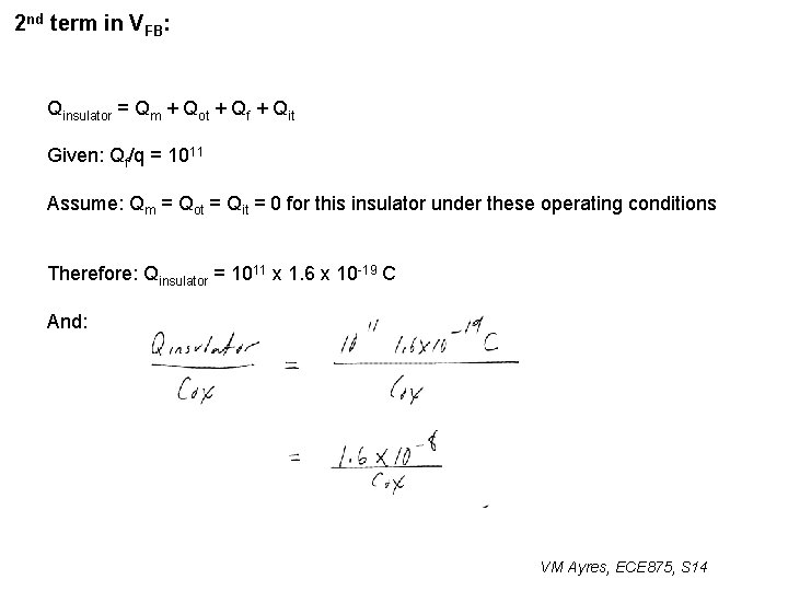
2 nd term in VFB: Qinsulator = Qm + Qot + Qf + Qit Given: Qf/q = 1011 Assume: Qm = Qot = Qit = 0 for this insulator under these operating conditions Therefore: Qinsulator = 1011 x 1. 6 x 10 -19 C And: VM Ayres, ECE 875, S 14

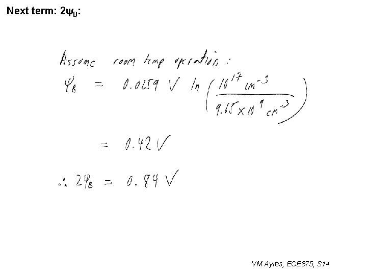
Next term: 2 y. B: VM Ayres, ECE 875, S 14

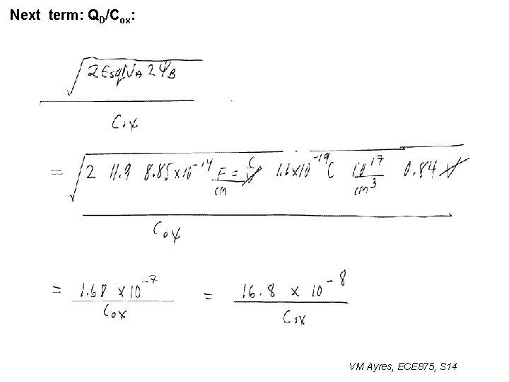
Next term: QD/Cox: VM Ayres, ECE 875, S 14

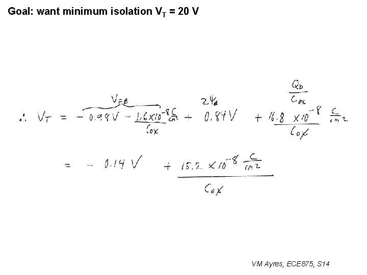
Goal: want minimum isolation VT = 20 V VM Ayres, ECE 875, S 14

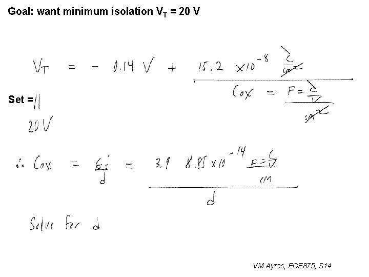
Goal: want minimum isolation VT = 20 V Set = VM Ayres, ECE 875, S 14

Lecture 36, 09 Apr 14 Chp 06: MOSFETs Aspects of realistic MOSFET operation (n-channel p-substrate) Comment on 2 D mobility m Use of field oxide in CMOS Short channel effects on ON operation: • high E (y) => velocity saturation => lower IDS • micron-scale = worst • nano-scale = not so bad • scaling Good test for future ON/OFF operation: sub-threshold (not fully ON) swing VM Ayres, ECE 875, S 14

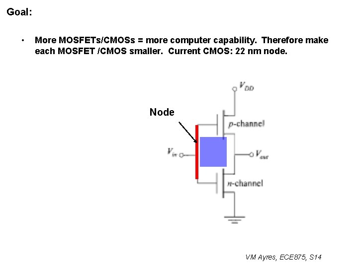
Goal: • More MOSFETs/CMOSs = more computer capability. Therefore make each MOSFET /CMOS smaller. Current CMOS: 22 nm node. Node VM Ayres, ECE 875, S 14

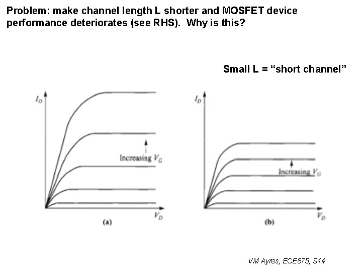
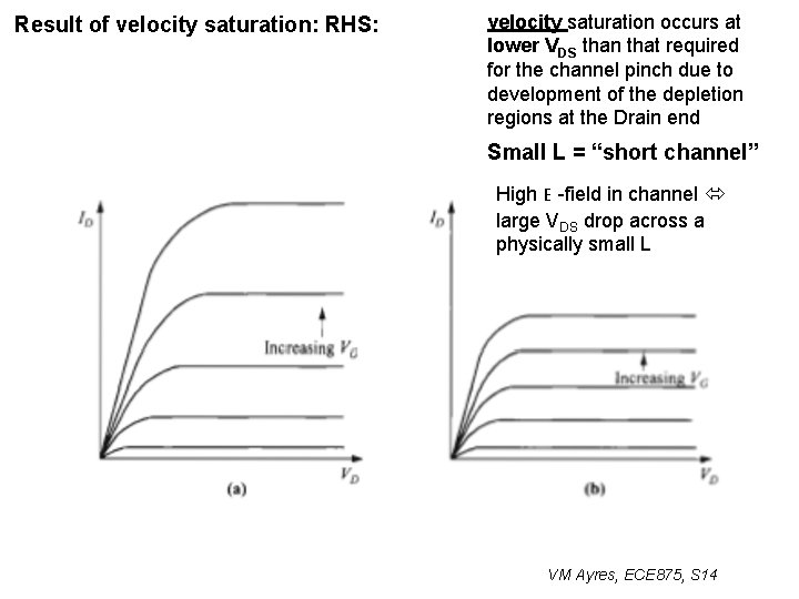
Problem: make channel length L shorter and MOSFET device performance deteriorates (see RHS). Why is this? Small L = “short channel” VM Ayres, ECE 875, S 14

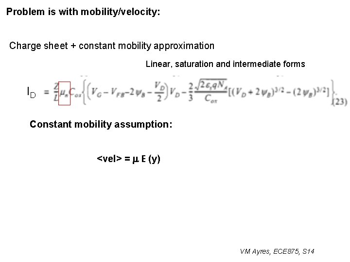
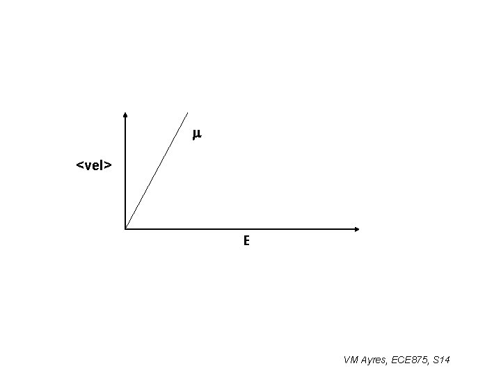
Problem is with mobility/velocity: Charge sheet + constant mobility approximation Linear, saturation and intermediate forms ID Constant mobility assumption: <vel> = m E (y) VM Ayres, ECE 875, S 14

m <vel> E VM Ayres, ECE 875, S 14

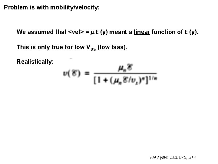
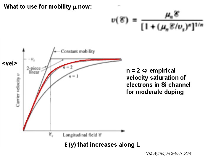
Problem is with mobility/velocity: We assumed that <vel> = m E (y) meant a linear function of E (y). This is only true for low VDS (low bias). Realistically: VM Ayres, ECE 875, S 14

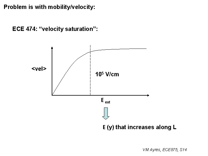
Problem is with mobility/velocity: ECE 474: “velocity saturation”: <vel> 105 V/cm E ext E (y) that increases along L VM Ayres, ECE 875, S 14

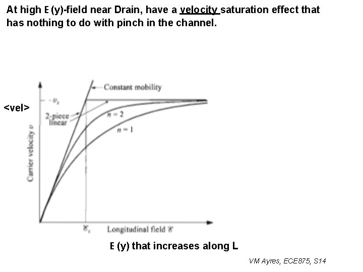
At high E (y)-field near Drain, have a velocity saturation effect that has nothing to do with pinch in the channel. <vel> E (y) that increases along L VM Ayres, ECE 875, S 14

Result of velocity saturation: RHS: velocity saturation occurs at lower VDS than that required for the channel pinch due to development of the depletion regions at the Drain end Small L = “short channel” High E -field in channel large VDS drop across a physically small L VM Ayres, ECE 875, S 14

What to use for mobility m now: <vel> n = 2 empirical velocity saturation of electrons in Si channel for moderate doping E (y) that increases along L VM Ayres, ECE 875, S 14

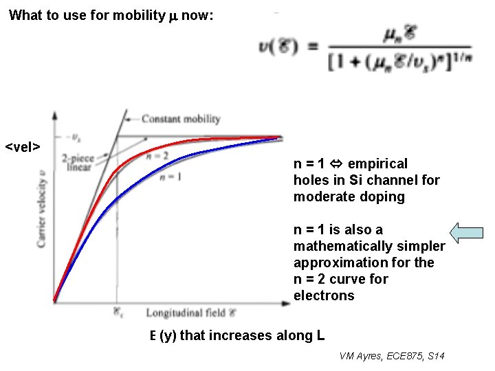
What to use for mobility m now: <vel> n = 1 empirical holes in Si channel for moderate doping n = 1 is also a mathematically simpler approximation for the n = 2 curve for electrons E (y) that increases along L VM Ayres, ECE 875, S 14

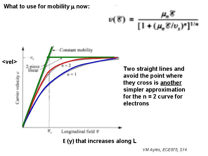
What to use for mobility m now: <vel> Two straight lines and avoid the point where they cross is another simpler approximation for the n = 2 curve for electrons E (y) that increases along L VM Ayres, ECE 875, S 14