Development of highperformance DLC resistive electrodes for MPGDs


: a class of metastable amorphous carbon material that contains both the")


 is ready to")

: a novel MPGD with resistive electrode and a single")


- Slides: 28
Development of high-performance DLC resistive electrodes for MPGDs You Lv , Yi Zhou , Jianbei Liu State Key Laboratory of Particle Detection and Electronics University of Science and Technology of China The 2019 International Workshop on the High Energy Circular Electron Positron Collider 18/11/2019 ---20/11/2019 1
Outline Ø Introduction Ø R&D on DLC resistive electrodes Ø Application of DLC coating 1. 2. 3. Low-rate μRWELL high-rate μRWELL Charging-up free THGEM Ø Summary 2
Development of MPGDs Advantages of MPGDs : • High rate capability (>> 1 MHz/cm 2) • Space resolution, mainly depending on the readout segmentation and FEE capability, easily below 200 μm • Time resolution below 10 ns • Larger area (m 2/single detector), lower cost MPGD technology are well established after more than 20 years of production at CERN, and it have already been widely studied and used in nuclear and particle physics experiments. 3
MPGDs applied in CEPC u Gas amplification detector module for CEPC TPC readout • • Baseline detector: GEM & MM Gain: 103− 104 Spatial granularity: 1 mm 2 Position resolution: 100 μm in r - φ u CEPC muon detector system • • • Candidate MPGD detector: μ-RWELL Sensitive area: 8600 m 2 Time resolution: 1 -2 ns Detector efficiency: 95% (Pμ >5 Ge. V) Rate capability: ~ 60 Hz/cm 2 4
Challenge in MPGDs: suffer discharge due to a large amount of avalanche charge created in a very narrow multiplication region. Resistive electrode based on Carbon loaded pastes have already been used in MPGDs to suppress the discharges and reduce the damaging effects on MPGDs × × Resistivity sometimes out of control in manufacture; Unable to make fine structures; Difficult to make conductive route on it precisely; Can not open opportunities for new micro-structures; New reliable resistive materials and preparation methods needed 5
Ø Introduction Ø R&D on DLC resistive electrodes Ø Application of DLC coating 1. 2. 3. Low-rate μRWELL high-rate μRWELL Charging-up free THGEM Ø Summary 6
Diamond-like Carbon (DLC): a class of metastable amorphous carbon material that contains both the diamond-structure and graphite-structure. Atom structure of DLC coating was firstly used in MSGC in 1995 to resolve the charging-up effect • DLC coating shows good stability in surface resistivity and good chemical stability. • Resistive electrodes based on DLC are very resistant to discharge and radiation, and able to withstand chemical or physical manufacturing processes. 7
R&D on DLC resistive electrodes Magnetron sputtering technique: an effective way for DLC coating at low-temperature, which ensures both accurate surface resistivity and uniform thickness of the coating. Schematic of magnetron sputtering technique 1. 2. 3. 4. Magnetron sputtering system (LICP Teer 650) Voltage between substrate and target ramping up Glow discharges appear, producing primary electrons and ions Ions hitting targets and sputtering carbons Ejected atoms depositing on substrate DLC coating deposited by Magnetron sputtering shows good adhesion and good uniformity. 8
Surface resistivity of DLC coating a-C DLC: pure DLC Surface resistivity: MΩ/□ — GΩ/□ Thickness: 50 nm — 100 nm a-C: H DLC: Hydrogen doping DLC Surface resistivity : MΩ/□ —TΩ/□ Thickness: 50 nm — 1μm Resistivity vs Vacuum a-c DLC a-c: H DLC • a-C DLC: Surface resistivity can be adjusted by initial vacuum degree and DLC thickness. • a-C: H DLC: The surface resistivity is sensitive to hydrogen, it can be adjusted in a very wide range by adjusting the ratio of hydrogen, and more precise by controlling deposition time. 9
Stability & uniformity • • Surface resistivity increase about 30% in 4 days (exposure to air), and then kept stable. Resistivity is independent with the voltage, showing the ohmic behavior. Carbon target • The resistivity uniformity better than 15% for 15 cm× 15 cm sample size, and 44% @30 cm × 30 cm DLC sample. • The height of carbon target is about 30 cm almost same as our large sample size. • DLC thickness showing difference at different region of the large DLC sample, which result to the bad uniformity. 210 200 178 176 200 105 93 96 82 102 68 70 72 71 68 78 77 78 81 77 135 130 120 135 126 10
Copper-coated DLC A copper-coated DLC is developed to extend the application of DLC coating in MPGDs. Cu layer Cr-Cu interlayer Cr layer DLC layer APICAL foil Substrate/DLC/Cr/Cr-Cu/Cu Copper-coated DLC Good adhesion 1. Deposit DLC on APICAL/Cu substrate 2. Deposit copper on DLC/APICAL/Cu substrate It shows good adhesion between DLC and copper. The thickness of copper can be adjusted from 1 μm to 5 μm. Further processing of the copper-coated DLC can be achieved thanks to the copper layer on the surface of DLC. Thickness measurment 11
R&D on larger DLC sample A new sputtering system (Hauzer 850) is ready to make larger area DLC samples. Picture of new sputtering system (Hauzer 850) 600 mm × 120 mm DLC sample Chamber size: Φ 800 mm× 900 mm Target size: 600 mm× 125 mm Resistivity uniformity: 25% @400 mm× 1200 mm DLC sample Resistivity shows good uniformity along the long edge, and bad on the short edge due to the limitation of target size. 12
Ø Introduction Ø R&D on DLC resistive electrodes Ø Application of DLC coating 1. 2. 3. Low-rate μRWELL high-rate μRWELL Charging-up free THGEM Ø Summary 13
Low-rate μRWELL Micro-Resistive WELL (μRWELL): a novel MPGD with resistive electrode and a single stage of well-type gas amplification. 1. Resistive electrode 2. One-stage WELL pattern ü Suppress discharge ü Compact and high granularity ü Fabrication fast μRWELL PCB: It is a stack of “readout PCB / insulating pre-preg / DLC resistive layer / welltype amplification” structure. A critical component of μRWELL PCB is DLC resistive electrode, which is used to suppress the discharge. μRWELL detector 14
2 -D μRWELL prototype • A 2 -D μRWELL detector prototype was designed and fabricated. • It is composed of a drift cathode and a μRWELL PCB which are fixed in a frame. • Drift region: 3 mm The μRWELL detector prototype was fully tested with X-rays/moun beam in Ar/CO 2 (70%/30%) gas mixture. μRWELL prototype 8 ke. V Cu X-rays Energy resolution: 21% @8 ke. V X-rays Gas gain: 1. 4× 10⁴ @500 V 15
Efficiency & position resolution Detection efficiency VS Voltage • Top layer: ~95%, Bottom layer: ~92% • Top & Bottom efficiency: ~90% Top induced charge is 1. 9 times of Bottom Position resolutions: Chargeweighted center of gravity method. Position resolution better than 70 μm achieved on both readout directions. Bottom layer Top/Bottom charge Efficiency vs Voltage Top layer 16
Rate capability The rate capability is assessed by measuring the detector gain as a function of counting rate per unit area. X-ray gun Source: 8 ke. V Copper x-ray Collimator: 5. 5 mm-diameter Normalized gain vs. Rate at different region Gain decreases about 10% @100 k. Hz/cm 2. Gain drop is still modest (<30%) @1 MHz/cm 2. The charge spreads on the DLC resistive electrode, inducing a current flowing through the resistive layer, generating a localized drop of the amplifying voltage, decreasing the gain. 17
High-rate μRWELL solution Two types of high-rate μRWELL solution are presented based on copper-coated DLC resistive electrode. Solution 1: 1 -DLC layer μRWELL with fast grounding lines. Solution 2: 2 -DLC layers μRWELL by SBU (Sequential Build Up). 5% Dead area 12 mm The copper clad on the DLC coating is etched to dash lines (100 μm width) and grounded, the electrons accumulated on DLC electrode can release faster. Reduce the path of the current on the DLC surface by implementing the first matrix of conductive vias connecting two stacked resistive layers. The second matrix conductive vias connects the second resistive layer to ground through the readout electrodes. 18
High-rate μRWELL PCB 1 -DLC layer 2 -DLC layers Grounding line Copper DLC 1. Two different high-rate μRWELL prototype have been designed and fabricated. 2. These μRWELL prototype are tested in Ar/CO 2 (70%/30%) gas mixture, showing a good response to X-rays, but a lower gas gain (~1000). Lower resistivity of DLC resistive electrode, weak suppress to discharge, lower gain. We are in close collaboration with Rui from CERN to optimize these detectors. 19
Charging-up free THGEM DLC is deposited on the dielectric surface of THGEM foil, in attempt to remove charging-up effect. Copper PCB DLC THGEM Gain vs. voltage DLC Gain vs. time The long term charging-up effect of DLC-THGEM is removed. 20
Summary 1. Performance and production process of DLC, as high quality resistive materials, have been studied based on magnetron sputtering technique. ü Surface resistivity: 1 MΩ/□~100 MΩ/□ @a-C ü Resistivity uniformity: <15% @15 cm× 15 cm MΩ/□~ TΩ/□ @a-C: H <25% @25 cm× 25 cm 2. The characterization of a 2 -D readout μRWELL based on DLC resistive electrode are performed. ü Gas gain: >104 2 -D position resolution: <70 μm @3 mm drift region ü 2 -D detection efficiency: >90% @3 mm drift region ü Rate capability: Gain drop 10% @100 k. Hz/cm 2, 30% @1 MHz/cm 2 3. Two different types of high-rate μRWELL based on copper-coated DLC and the DLC-THGEM for charging-up free are presented too. Next step a) Exploring the larger DLC sample with new sputtering system (Hauzer 850). b) Optimizing the high-rate μRWELL prototype. 21
BACKUP 22
2 -D μRWELL PCB A 2 -D μRWELL PCB with 15 cm× 15 cm a-C DLC was designed and fabricated. Schematic of μRWELL PCB • Sensitive area: 10 cm× 10 cm divided into 4 sectors • Well pitch: 140 μm • Pre_preg (50 μm) isolate the DLC electrode from readout strip • • • Readout strip pitch: 400 μm Top layer: 80 μm Bottom layer: 350 μm Readout strip channel: 512 Distance (Top to Bottom layer): 50 μm μRWELL PCB All the readout strips are connected to 4 HIROSE (for laboratory test) and 4 PANASONIC (for beam test) connectors. 23
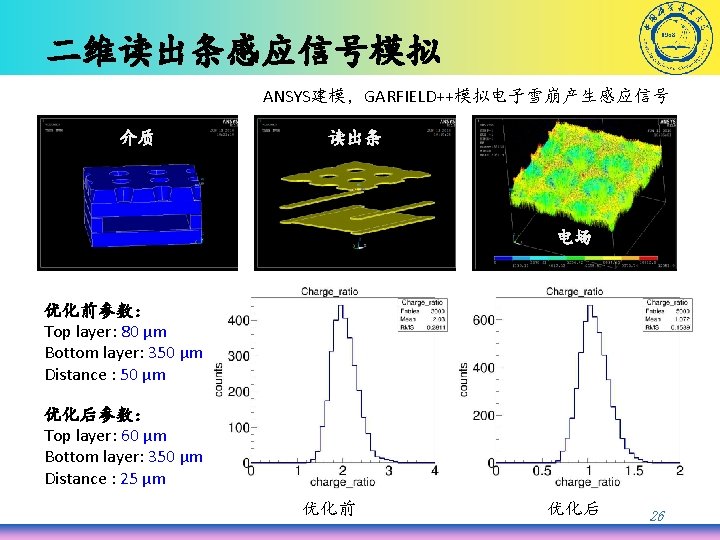
Optimization of 2 -D readout strip Achieving an equivalent induced signal on the 2 -D readout strips. 1. Detector’s geometry & Electric field map are resolved by ANSYS. 2. Induced signal is exported from GARFIELD++ by simulating single electron avalanching. • • • Before Top layer: 80 μm Bottom layer: 350 μm Distance : 50 μm Top layer Bottom layer • • • NOW Top layer: 60 μm Bottom layer: 350 μm Distance : 25 μm • Increase strip width of bottom layer and decrease strip width of top layer. • The energy spectrum peak of top layer almost same with bottom layer after optimization. Copper Spectrum after optimization of 2 -D readout strip Bottom/Top Copper/Bottom Sector 1 1. 09 2. 03 Sector 2 1. 11 1. 95 Sector 3 1. 14 2. 06 Sector 4 1. 11 1. 95 Peak ratio in different sector 24
The charge spread on the DLC resistive electrode, inducing a current flowing through the resistive layer, generates a localized drop of the amplifying voltage, decreased the gain. 25
优化后测试结果 Ar/CO 2=70/30 8 ke. V copper X-rays Top layer Bottom layer Copper Gain Sector 1能谱 Bottom/Top Copper/Bottom Sector 1 1. 09 2. 03 Sector 2 1. 11 1. 95 Sector 3 1. 14 2. 06 Sector 4 1. 11 1. 95 Energy spectrum peak at different sector 27
28