DEPFET Prototype System for the ILC Vertex detector
- Slides: 18

DEPFET Prototype System for the ILC Vertex detector: First test beam results Lars Reuen, 7 th Conference on Position Sensitive Devices, Liverpool Univ. of Bonn: M. Karagounis, R. Kohrs, H. Krüger, L. Reuen, C. Sandow, E. von Törne, M. Trimpl, J. Velthuis, N. Wermes Univ. of Mannheim: P. Fischer, F. Giesen, I. Peric MPI Halbleiterlabor Munich: L. Andricek, G. Lutz, H. G. Moser, R. H. Richter, M. Schnecke, L. Strüder, J. Treis, P. Lechner 12. Sep. 2005 Lars Reuen, PSD 2005 Liverpool

Overview • Reminder – ILC requirements – DEPFET principle of operation – DEPFET ILC prototype system • Material Budget Power dissipation • First Test Beam Results 12. Sep. 2005 Lars Reuen, PSD 2005 Liverpool 2

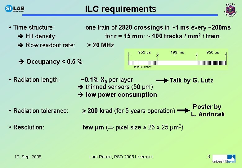
ILC requirements • Time structure: Hit density: Row readout rate: one train of 2820 crossings in ~1 ms every ~200 ms for r = 15 mm: ~ 100 tracks / mm 2 / train > 20 MHz Occupancy < 0. 5 % • Radiation length: ~0. 1% X 0 per layer thinned sensors (50 μm) low power consumption Talk by G. Lutz • Radiation tolerance: 200 krad (for 5 years operation) • Resolution: few µm ( pixel size ≤ 25 x 25 µm 2) 12. Sep. 2005 Lars Reuen, PSD 2005 Liverpool Poster by L. Andricek 3

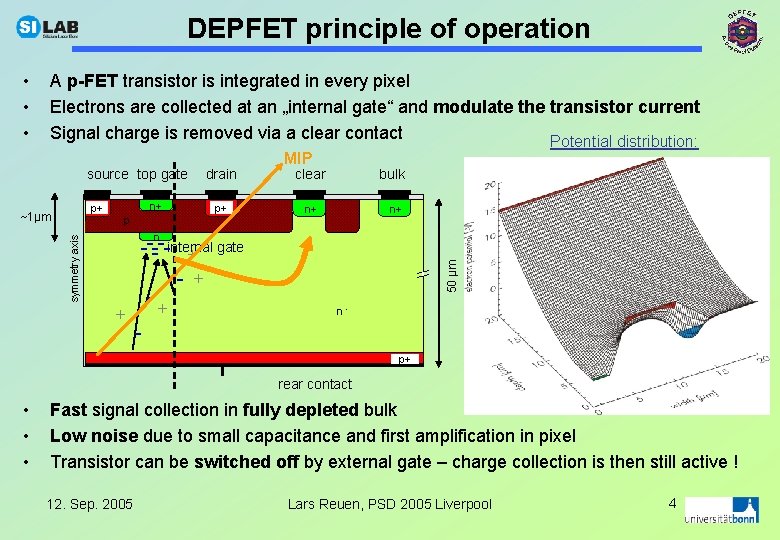
DEPFET principle of operation A p-FET transistor is integrated in every pixel Electrons are collected at an „internal gate“ and modulate the transistor current Signal charge is removed via a clear contact Potential distribution: source top gate p+ n+ p+ p symmetry axis ~1µm drain + n gate ------internal + -+ - MIP clear bulk n+ n+ 50 µm • • • n- p+ rear contact • • • Fast signal collection in fully depleted bulk Low noise due to small capacitance and first amplification in pixel Transistor can be switched off by external gate – charge collection is then still active ! 12. Sep. 2005 Lars Reuen, PSD 2005 Liverpool 4

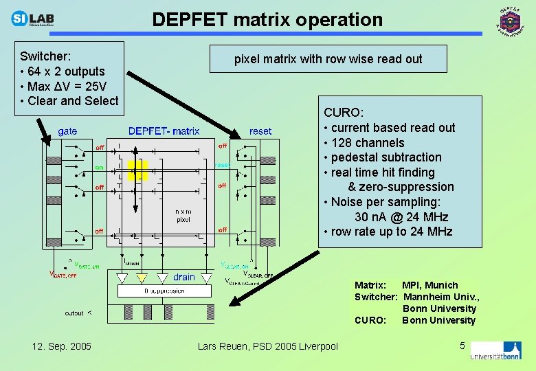
DEPFET matrix operation Switcher: • 64 x 2 outputs • Max ΔV = 25 V • Clear and Select pixel matrix with row wise read out CURO: • current based read out • 128 channels • pedestal subtraction • real time hit finding & zero-suppression • Noise per sampling: 30 n. A @ 24 MHz • row rate up to 24 MHz Matrix: MPI, Munich Switcher: Mannheim Univ. , Bonn University CURO: Bonn University 12. Sep. 2005 Lars Reuen, PSD 2005 Liverpool 5

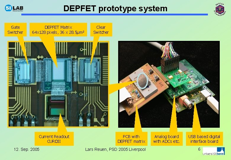
DEPFET prototype system Gate Switcher DEPFET Matrix 64 x 128 pixels, 36 x 28. 5µm 2 Current Readout CUROII 12. Sep. 2005 Clear Switcher PCB with DEPFET matrix Lars Reuen, PSD 2005 Liverpool Analog board with ADCs etc. USB based digital interface board 6

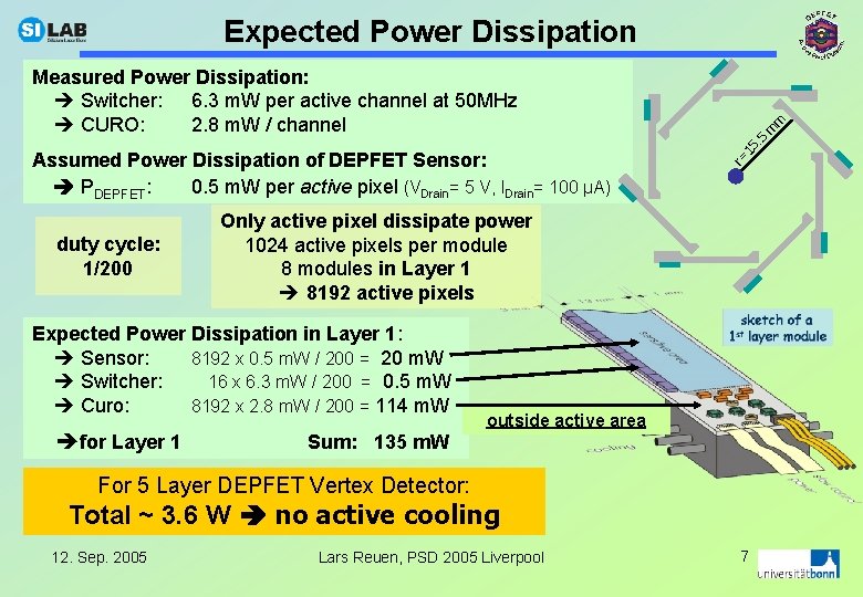
Expected Power Dissipation Assumed Power Dissipation of DEPFET Sensor: PDEPFET: 0. 5 m. W per active pixel (VDrain= 5 V, IDrain= 100 µA) duty cycle: 1/200 Only active pixel dissipate power 1024 active pixels per module 8 modules in Layer 1 8192 active pixels Expected Power Dissipation in Layer 1: Sensor: 8192 x 0. 5 m. W / 200 = 20 m. W Switcher: 16 x 6. 3 m. W / 200 = 0. 5 m. W Curo: 8192 x 2. 8 m. W / 200 = 114 m. W for Layer 1 r= 15 . 5 m m Measured Power Dissipation: Switcher: 6. 3 m. W per active channel at 50 MHz CURO: 2. 8 m. W / channel outside active area Sum: 135 m. W For 5 Layer DEPFET Vertex Detector: Total ~ 3. 6 W no active cooling 12. Sep. 2005 Lars Reuen, PSD 2005 Liverpool 7

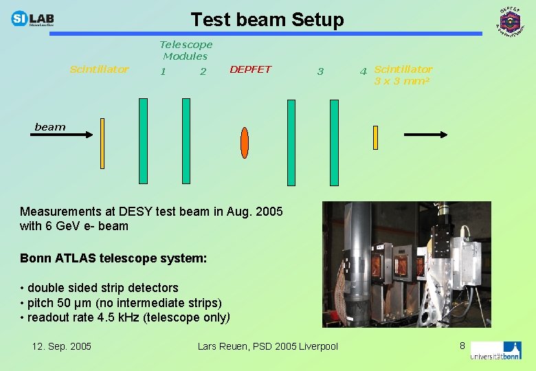
Test beam Setup Telescope Modules Scintillator 1 2 DEPFET 3 4 Scintillator 3 x 3 mm² beam Measurements at DESY test beam in Aug. 2005 with 6 Ge. V e- beam Bonn ATLAS telescope system: • double sided strip detectors • pitch 50 µm (no intermediate strips) • readout rate 4. 5 k. Hz (telescope only) 12. Sep. 2005 Lars Reuen, PSD 2005 Liverpool 8

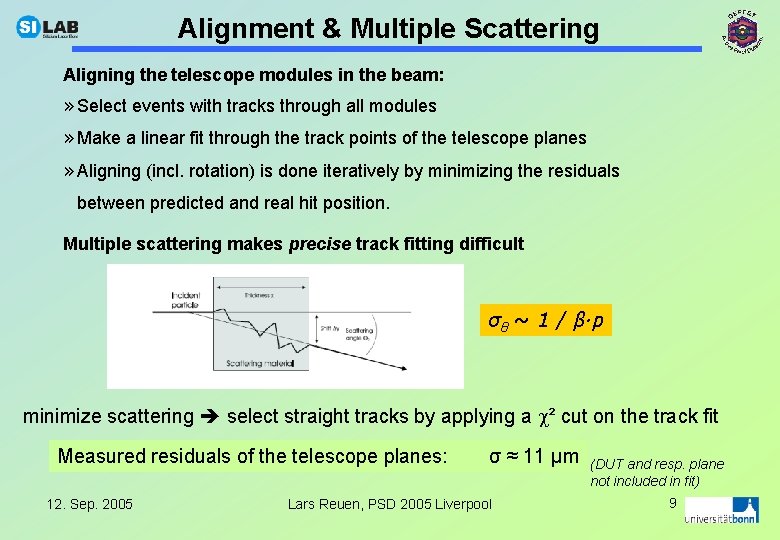
Alignment & Multiple Scattering Aligning the telescope modules in the beam: » Select events with tracks through all modules » Make a linear fit through the track points of the telescope planes » Aligning (incl. rotation) is done iteratively by minimizing the residuals between predicted and real hit position. Multiple scattering makes precise track fitting difficult σθ ~ 1 / β∙p minimize scattering select straight tracks by applying a ² cut on the track fit Measured residuals of the telescope planes: 12. Sep. 2005 σ ≈ 11 µm Lars Reuen, PSD 2005 Liverpool (DUT and resp. plane not included in fit) 9

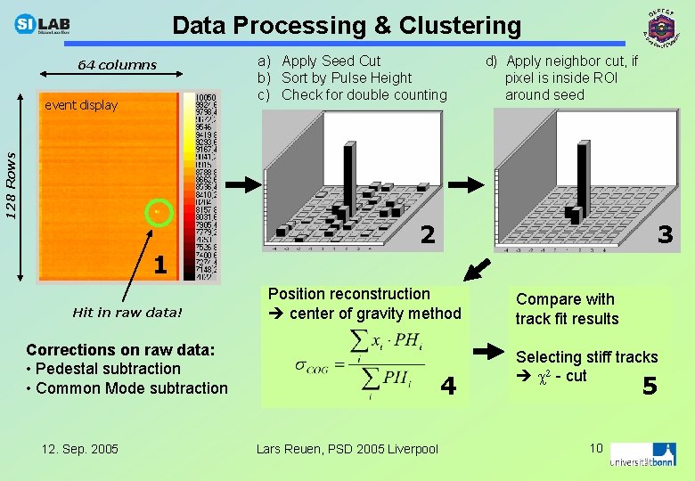
Data Processing & Clustering 64 columns 128 Rows event display a) Apply Seed Cut b) Sort by Pulse Height c) Check for double counting d) Apply neighbor cut, if pixel is inside ROI around seed 2 3 1 Hit in raw data! Position reconstruction center of gravity method Corrections on raw data: • Pedestal subtraction • Common Mode subtraction 12. Sep. 2005 4 Lars Reuen, PSD 2005 Liverpool Compare with track fit results Selecting stiff tracks 2 - cut 5 10

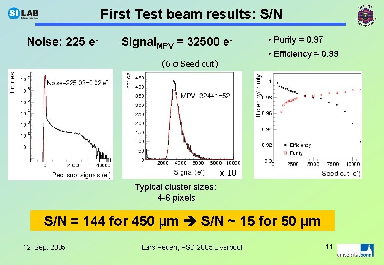
First Test beam results: S/N Noise: 225 e- Signal. MPV = 32500 e- • Purity ≈ 0. 97 • Efficiency ≈ 0. 99 (6 σ Seed cut) x 10 Typical cluster sizes: 4 -6 pixels S/N = 144 for 450 µm S/N ~ 15 for 50 µm 12. Sep. 2005 Lars Reuen, PSD 2005 Liverpool 11

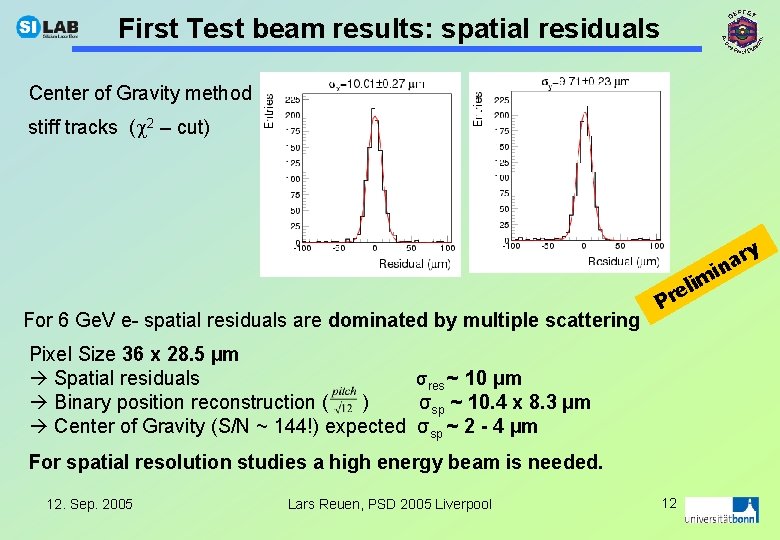
First Test beam results: spatial residuals Center of Gravity method stiff tracks ( 2 – cut) y m li re For 6 Ge. V e- spatial residuals are dominated by multiple scattering P Pixel Size 36 x 28. 5 µm Spatial residuals σres ~ 10 μm Binary position reconstruction ( ) σsp ~ 10. 4 x 8. 3 µm Center of Gravity (S/N ~ 144!) expected σsp ~ 2 - 4 µm For spatial resolution studies a high energy beam is needed. 12. Sep. 2005 Lars Reuen, PSD 2005 Liverpool 12 r a n i

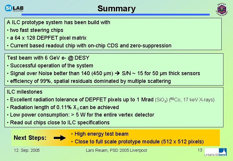
Summary A ILC prototype system has been build with • two fast steering chips • a 64 x 128 DEPFET pixel matrix • Current based readout chip with on-chip CDS and zero-suppression Test beam with 6 Ge. V e- @ DESY • Successful operation of the system • Signal over Noise better than 140 (450 µm) S/N ~ 15 for 50 µm thick sensors • efficiency of 99%, spatial residuals dominated by multiple scattering ILC milestones • Excellent radiation tolerance of DEPFET pixels up to 1 Mrad (Si. O 2) (60 Co, 17 ke. V X-rays) • Radiation length of 0. 11% X 0 can be achieved • Low power consumption: > 5 W for the entire vertex detector • Read out chips close to ILC specifications Next Steps: 12. Sep. 2005 • High energy test beam • Close to full scale prototype module (512 x 512 pixels) Lars Reuen, PSD 2005 Liverpool 13

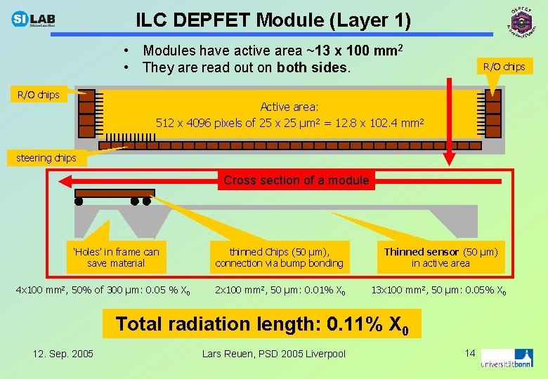
ILC DEPFET Module (Layer 1) • Modules have active area ~13 x 100 mm 2 • They are read out on both sides. R/O chips Active area: 512 x 4096 pixels of 25 x 25 µm 2 = 12. 8 x 10². 4 mm 2 steering chips Cross section of a module ‘Holes’ in frame can save material 4 x 100 mm 2, 50% of 300 μm: 0. 05 % X 0 thinned Chips (50 µm), connection via bump bonding Thinned sensor (50 µm) in active area 2 x 100 mm 2, 50 μm: 0. 01% X 0 13 x 100 mm 2, 50 μm: 0. 05% X 0 Total radiation length: 0. 11% X 0 12. Sep. 2005 Lars Reuen, PSD 2005 Liverpool 14

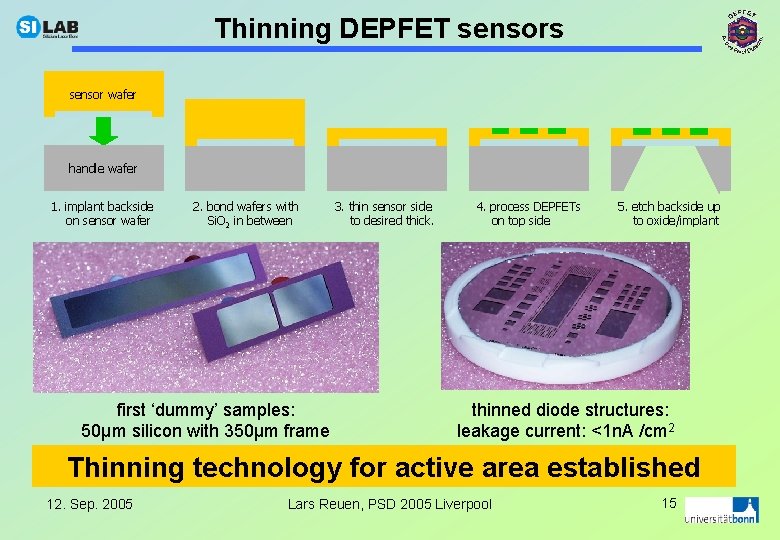
Thinning DEPFET sensors sensor wafer handle wafer 1. implant backside on sensor wafer 2. bond wafers with Si. O 2 in between first ‘dummy’ samples: 50µm silicon with 350µm frame 3. thin sensor side to desired thick. 4. process DEPFETs on top side 5. etch backside up to oxide/implant thinned diode structures: leakage current: <1 n. A /cm 2 Thinning technology for active area established 12. Sep. 2005 Lars Reuen, PSD 2005 Liverpool 15

Backup I: 12. Sep. 2005 Lars Reuen, PSD 2005 Liverpool 16

Backup II: 12. Sep. 2005 Lars Reuen, PSD 2005 Liverpool 17

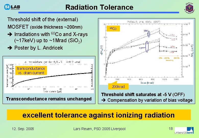
Radiation Tolerance Threshold shift of the (external) MOSFET (oxide thickness ~200 nm) Irradiations with 60 Co and X-rays (~17 ke. V) up to ~1 Mrad (Si. O 2) Poster by L. Andricek 60 Co transconductance vs. drain current 200 krad Transconductance remains unchanged Threshold shift saturates at -5 V (OFF) Compensation by variation of bias voltage excellent tolerance against ionizing radiation 12. Sep. 2005 Lars Reuen, PSD 2005 Liverpool 18