Dale Wheat Dallas Makerspace February 2019 Product of

Dale Wheat Dallas Makerspace February 2019

§ Product of STMicroelectronics • st. com § A family of 32 -bit Flash microcontrollers § Based on Arm® Cortex®-M processors • arm. com

§ Cortex-M 3 announced by ARM Holdings in 2004 § ARM Cortex-M uses ARMv 7 -M microarchitecture (not to be confused with ARM 7 devices) § First devices to market were Luminary Micro LM 3 S 101 & LM 3 S 102

§ Cortex-M 0+ § Cortex-M 1 § Cortex-M 3 § Cortex-M 4 § Cortex-M 7 § Cortex-M 23 § Cortex-M 35 P

§ What is STM 32 § How to use STM 32 -specific development software § How to program simple embedded programs in C § How to debug your programs § How to use code generator (STM 32 Cube. MX) for more complex projects § How to add simple peripherals to STM 32

§ A brief introduction to STM 32 § An understanding of how it compares to other available solutions § Access to STM 32 -specific development software § Sources for STM 32 hardware § Optional: Your very own STM 32 experimenter’s starter kit

§ Yes § A microcontroller executes user’s programs § Small form factor § Low cost § Modern tools make it simple to learn and use § Widely documented on the Internet § No § Arduino is based on Atmel AVR 8 -bit architecture at 16 MHz § STM 32 is based on Arm® Cortex®-M 32 -bit architecture at 32 MHz to 400 MHz § Not all STM 32 software is open source

§ Check your kit for the following items: § Solderless breadboard containing: § STM 32 “Blue Pill” board § ST-LINK V 2 USB interface § Four push buttons § Rainbow-colored jumper wires § USB to TTL serial adapter § USB cable (A to Micro-B) § Bag of LEDs and resistors § LCD module

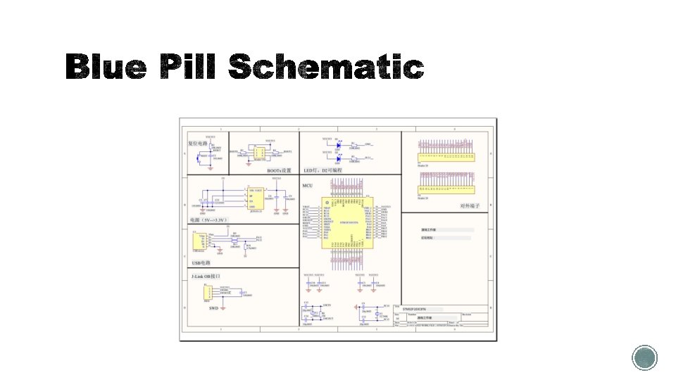
§ Low cost, generic ARM development module § Based on STM 32 F 103 C 8 T 6 § 40 pin DIP (dual in-line package) § Headers are usually optional
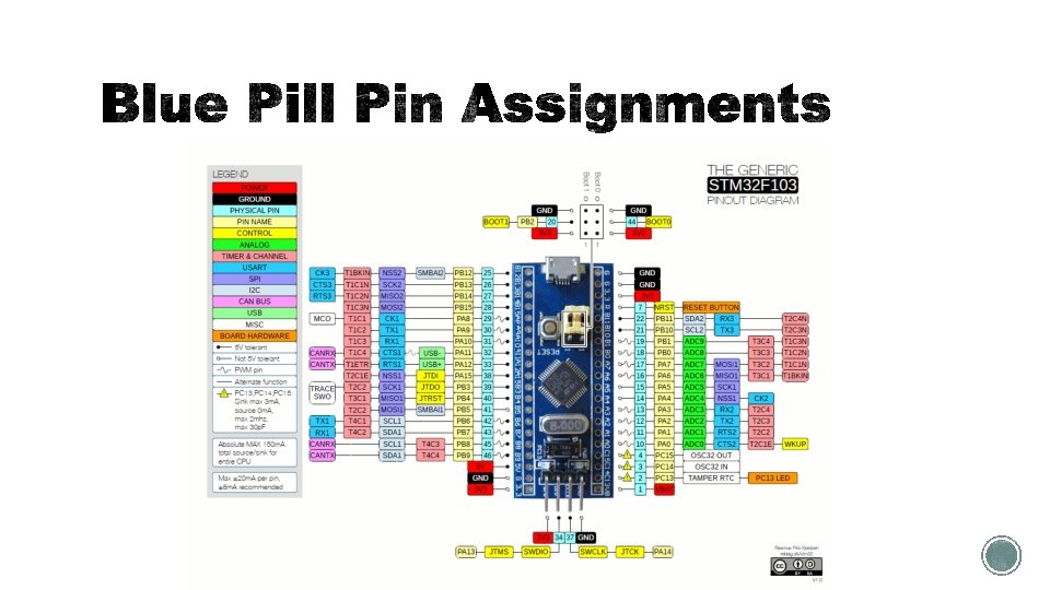
 § GND – ground reference § SWCLK")
§ Connection to blue pill (4 wires) § GND – ground reference § SWCLK – clock § SWDIO – data § 3 V 3 – 3. 3 V power

§ Spring-loaded sockets hold wires in place § Red lines indicate electrical connections

§ Always unplug the ST-LINK from the USB port when making wiring updates. § Do not add or remove components when board is powered on.

§ There is no console § Blink built-in LED on GPIO pin PC 13 § No jumpers required for this experiment § Connect ST-LINK/V 2 device to USB port § Observe fast blink rate of PC 13 (~5 Hz)

§ Click on Atollic True. STUDIO icon § Select workspace folder, if prompted § Close “Information Center” window, if displayed § Select “File/New/C Project…” menu item § In “Project name: ” field, enter “blink” § Select “Project type: ” as “Embedded C Project” § Click “Next >” button

§ Type “STM 32 F 103” in “Target” field § Select “STM 32 F 103 C 8” in Device list § Click “Next >” button

§ Click “Next >” button

§ For “Debug Probe” select “ST-LINK” § Click “Finish” button § “Build project” dialog appears while project is being built

§ Browse through all the system-generated code § “Libraries” contains useful system code § CMSIS is ARM standard code for Cortex-M devices § STM 32 F 10 x_Std. Periph_Driver contains ST-specific hardware libraries § “src” contains the source code for the project § “main. c” is the entry point for the project’s code

§ Line 32 contains the following code: “#include “stm 32 f 10 x. h” § Copy this line to the clip board § Method 1: § Highlight the line with the mouse § Right-click for context menu and select “Copy” § Method 2: § Highlight the line using the cursor keys § Move cursor to first part of line § Use “Shift+End” to highlight to end of line § Type Control+C

§ Type Control-A to select all § Press the “Delete” key § Add line 32 back into the source code for main. c § Method 1: Right-click and select “Paste” § Method 2: Type Control-V § Type “int main(void) {“ and press [Enter] § Editor adds closing bracket automatically § Click “Build ‘Debug’ for project ‘blink’” icon (hammer) § Review console output § Click on “Terminate” icon to end debugging session
 function: RCC->APB 2 ENR = RCC_APB")
§ Add the following code within the main() function: RCC->APB 2 ENR = RCC_APB 2 ENR_IOPCEN; // enable GPIO port C GPIOC->CRH = GPIO_CRH_MODE 13; // PC 13 = output, 50 MHz while(1) { GPIOC->BSRR = GPIO_BSRR_BS 13; // LED off GPIOC->BRR = GPIO_BRR_BR 13; // LED on }

§ Click on the Build icon § If “Save and Launch” dialog appears, check “Always save…”, then click “OK” button § Click on the Debug icon § Make sure “ST-LINK” is selected as the debugging device § The program is compiled and downloaded to the STM 32 chip § The debugger is started § Execution is halted just inside the main() function § Step over each line of code: § Method 1: Click the “Step Over” icon § Method 2: Press the F 6 button § Run the program full speed: § Method 1: Click the “Resume” icon (green arrow/play button) § Method 2: Press the F 8 button
: § for(int")
§ After the LED commands, add the following code (in two places): § for(int i = 0; i < 1000000; i++); § Your while() loop should now look like this: while(1) { GPIOC->BSRR = GPIO_BSRR_BS 13; // LED off for(int i = 0; i < 1000000; i++); GPIOC->BRR = GPIO_BRR_BR 13; // LED on for(int i = 0; i < 1000000; i++); } § Build and debug § Click “Terminate” icon to end debug session

§ Start the STM 32 Cube. MX program § Under “New Project”, click “ACCESS TO MCU SELECTOR” button § Under “Part Number Search”, enter “stm 32 f 103 c 8” § In “MCU List”, select “STM 32 F 103 C 8” line § Click “Start Project” button § STM 32 Cube. MX workspace screen is displayed § Use Zoom In, Zoom Out and Best Fit to resize image of chip

§ Under “System Core”, select “SYS” § Under “Debug”, select “Serial Wire” § Note that PA 13 and PA 14 pins are now green and labeled § In search box, enter “PC 13” § Pin PC 13 starts blinking § Click on PC 13 pin § Select “GPIO_Output” § Right-click on PC 13 pin § Select “Enter User Label” § Enter “LED” and press [Enter]
 § Click “GPIO” button § Select")
§ Select “System View” (instead of Pinout View) § Click “GPIO” button § Select “PC 13 -TAMPER-RTC” line § Change “GPIO output level” to “High”

§ Click “Project Manager” tab § In “Project Name” field, enter “blink 2” § In “Project Location” field, click “Browse” button § Select workspace folder in STM 32 folder § For “Toolchain / IDE”, select “True. STUDIO” § Click “GENERATE CODE” button § Click “Open Project” button

§ Return to True. STUDIO § Expand “blink 2” project in “Project Explorer” § Open “main. c” file in “Src” folder § Add your own code between “/* USER CODE BEGIN xxx *” and “/* USER CODE END xxx */” comments

§ Right-click “blink 2” in Project Explorer § Select “Properties” § Select “C/C++ Build / Settings” § Select “Tool Settings” tab § Select “C Compiler / Optimization” § For “Optimization Level” select “None (-O 0)” § Click the “OK” button
; §")
§ Look at line 173 in main. c: § HAL_GPIO_Write. Pin(LED_GPIO_Port, LED_Pin, GPIO_PIN_SET); § Copy this line to the clipboard § Go to line 120: /* USER CODE BEGIN 3 */ § After line 120, paste the code from line 173 § Paste it a second time § Modify the second copy from …_SET to …_RESET: § HAL_GPIO_Write. Pin(LED_GPIO_Port, LED_Pin, GPIO_PIN_RESET);

§ Build project § Debug § Use “Step Over” to trace program execution § Verify LED comes on when pin is reset, goes off when pin is set § Click “Resume” to run at full speed § Click “Suspend” to start debugging again § Click “Step Return” if needed to return to main() § Click “Terminate” to stop debugging
; §")
§ Add delays using HAL function after lines 121 and 122: § HAL_Delay(250); § Compile and debug § Verify expected operation
")
§ Select one of the LEDs from the kit package (red, green or blue) § Get one of the included resistors from the LED package § Install the LED and resistor per live demonstration § Add jumper wire from GPIO pin A 0 to LED anode § Use resistor as jumper from LED cathode to breadboard ground rail

§ Return to STM 32 Cube. MX program § Select “Pinout & Configuration” tab § Select “Pinout View” § Type “PA 0” into search tool § GPIO pin A 0 blinks on the screen § Click on PA 0 pin § Select “GPIO_Output” § Right-click on PA 0 pin and select “Enter User Label” § Enter “LED 2” and press [Enter]

§ Click “GENERATE CODE” button § Return to True. STUDIO § Copy line 121: § HAL_GPIO_Write. Pin(LED_GPIO_Port, LED_Pin, GPIO_PIN_SET); § Paste as line 122 § Change “LED” to “LED 2” in two places: § HAL_GPIO_Write. Pin(LED 2_GPIO_Port, LED 2_Pin, GPIO_PIN_SET); § Copy this line and paste it as line 125 § Change “_SET” to “_RESET”: § HAL_GPIO_Write. Pin(LED 2_GPIO_Port, LED 2_Pin, GPIO_PIN_RESET);
” § Verify new LED behaves")
§ Build § Debug using “Step Over (F 6)” § Verify new LED behaves as expected § Click “Resume (F 8)” to run at full speed § Click “Terminate” to end debugging session

§ Return to STM 32 Cube. MX § Click on PA 0 pin, select “TIM 2_CH 1” § Right-click pin PA 0, select “Enter User Label”, enter “LED 2” § Under “Timers” select “TIM 2” § For “Clock Source”, select “Internal Clock” § For “Channel 1”, select “PWM Generation CH 1” § Under “Prescaler”, enter “ 65000” § For “Counter Period”, enter “ 123” § For “Pulse”, enter “ 30” § Click the “GENERATE CODE” button

§ Timers do not start automatically § After line 113 (“/* USER CODE BEGIN 2 */”), add: § HAL_TIM_PWM_Start(&htim 2, TIM_CHANNEL_1); § Build § Debug § Verify LED 2 operation § Note that the GPIO functions no longer affect LED 2

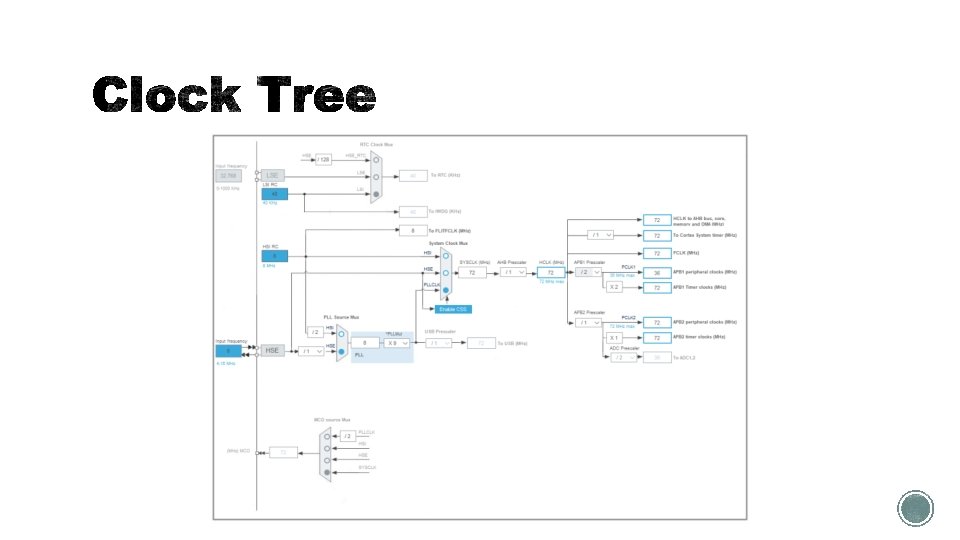
§ After boot, the STM 32 F 103 runs on an internal RC oscillator (HSI) at ~8 MHz § The Blue Pill contains an 8 MHz quartz crystal with much better speed tolerance § Return to STM 32 Cube. MX § On “Pinout & Configuration” tab, select “RCC” § For “High Speed Clock (HSE)”, select “Crystal/Ceramic Resonator” § Go to “Clock Configuration” tab § For “PLL Source Mux”, select “HSE” § For “*PLLMul”, select “X 9” § For “System Clock Mux”, select “PLLCLK” § For “APB 1 Prescaler”, select “/ 2”

§ Click “GENERATE CODE” button § Return to True. STUDIO § Build § Debug § Click “Resume” icon to run at full speed § Note faster blinking of LED 2 § Note that LED is still flashing at the same rate § This is because the HAL_Delay() function knows the CPU frequency

§ Connect jumper from GPIO pin A 1 to pin on yellow push button § Return to STM 32 Cube. MX § On “Pinout & Configuration” tab, on the “Pinout View”, search for pin PA 1 § All matching pins begin to blink § Click on pin PA 1 and select “GPIO_Input” § Right-click on pin PA 1, select “Enter User Label” and enter “button” § Select “System View” tab and click on “GPIO” button § Click on “PA 1” line § For “GPIO Pull-up/Pull-down”, select “Pull-up” § Click “GENERATE CODE” button

§ Return to True. STUDIO § Add the following code after line 133: if(HAL_GPIO_Read. Pin(button_GPIO_Port, button_Pin) == GPIO_PIN_RESET) { TIM 2 ->CCR 1 = 60; } else { TIM 2 ->CCR 1 = 0; } § Build § Debug § Test effects of button presses on LED 2’s output

§ USART = Universal Synchronous/Asynchronous Receiver/Transmitter § The STM 32 F 103 C 8 has three (3) USARTs § USART 1 § USART 2 § USART 3
")
§ Install USB-TTL adapter on breadboard as shown on the screen § Ground (GND) connection is already made via the breadboard power rail § Use a jumper to connect pin labeled RXD to PA 9 § Use another jumper to connect pin labeled TXD to PA 10

§ Return to STM 32 Cube. MX § Under “Connectivity”, select “USART 1” § For “Mode”, select “Asynchronous” § Click the “GENERATE CODE” button § Click the “Open Project” button
 loop: uint 8_t buffer; if(HAL_UART_Receive(&huart 1,")
§ Add this code in main. c’s while() loop: uint 8_t buffer; if(HAL_UART_Receive(&huart 1, &buffer, 1, 100) == HAL_OK) { HAL_UART_Transmit(&huart 1, &buffer, 1, 500); // echo it } § Build § Debug § Click “Resume” icon to run at full speed

§ If “Terminal” pane is not visible: § Select “Window / Show View / Terminal” menu item § Click the “Open a Terminal” icon § In the “Launch Terminal” dialog box: § For “Choose terminal: ”, select “Serial Terminal” § For “Port: ”, select correct port (usually the highest numbered port) § For “Baud Rate: ”, select “ 115200” § Click the “OK” button § Start typing in the Terminal window § Verify characters are being echoed back correctly
 device")
§ STM 32 F 103 C 8 device supports USB Full Speed (FS) device § STM 32 Cube. MX will supply basic code for six (6) types of device classes: § Audio § Communication (virtual serial port) § Download Firmware Update (DFU) § Human Interface Device (HID) § Custom Human Interface Device § Mass Storage § Step by step video for setting up a USB CDC: § https: //www. youtube. com/watch? v=YZjn. COun 1 w. U

§ Return to STM 32 Cube. MX § Under “Connectivity”, click on “USB” § Check “Device (FS)” § Under “Middleware”, select “USB_DEVICE” § For “Class For FS IP”, select “Communication Device Class (Virtual Port Com)” § Go to “Clock Configuration” tab § For “USB Prescaler”, select “/ 1. 5” § Click the “GENERATE CODE” button § Click “Close”
, add: #include \"usbd_cdc_if. h“")
§ After line 56 (“/* USER CODE BEGIN Includes */”), add: #include "usbd_cdc_if. h“ § After line 124 (“/* USER CODE BEGIN 2 */”), add: HAL_Delay(1000); CDC_Transmit_FS((uint 8_t *)"Hello, worldrn", 14); § Within the main() function’s while() loop, add: HAL_GPIO_Write. Pin(LED_GPIO_Port, LED_Pin, GPIO_PIN_RESET); // LED on CDC_Transmit_FS((uint 8_t *)"Tickrn", 6); HAL_Delay(250); HAL_GPIO_Write. Pin(LED_GPIO_Port, LED_Pin, GPIO_PIN_SET); // LED off CDC_Transmit_FS((uint 8_t *)"Tockrn", 6); HAL_Delay(250);
, add:")
§ In usbd_cdc_if. c, after line 293 (“/* USER CODE BEGIN 6 */”), add: if(Buf[0] == '1') { HAL_GPIO_Write. Pin(LED 2_GPIO_Port, LED 2_Pin, GPIO_PIN_SET); // LED 2 on CDC_Transmit_FS((uint 8_t *)"LED onrn", 8); } else { HAL_GPIO_Write. Pin(LED 2_GPIO_Port, LED 2_Pin, GPIO_PIN_RESET); // LED 2 off CDC_Transmit_FS((uint 8_t *)"LED offrn", 9); }

§ Connect the Blue Pill to your PC using the USB cable § Build the project § Debug § Terminate § Unplug and re-plug the USB cable from the Blue Pill § User Device Manager to determine the COM port number of the Virtual Serial Port § If required, install the virtual serial port device driver § Open a serial terminal and configure for the proper serial port § Unplug the ST-LINK/V 2 device § Unplug and re-plug the USB cable to the Blue Pill § Verify operation

§ Note: This is an extra credit experiment § Remove smaller static-dissipative bag containing LCD from kit § Note: Smaller bag contains both the LCD and a small resistor § Install the LCD on the breadboard as shown on screen § Only twelve (12) of the sixteen (16) LCD connections are required
 to ground rail § Connect 5. 0 V")
§ Connect LCD pin 1 (VSS) to ground rail § Connect 5. 0 V pin on ST-LINK/V 2 to lower-left power rail § Connect LCD pin 2 (VDD) to 5. 0 V rail § Connect LCD pin 3 (VO) to ground using 2. 0 KΩ resistor § Apply power to circuit § Confirm LCD displays a single row of white boxes
 to 5. 0 V rail via resistor from")
§ Connect LCD pin 15 (A) to 5. 0 V rail via resistor from LED bag § Connect LCD pin 16 (K) t o ground rail § Apply power to circuit § Verify that backlight is illuminated
 to pin PA 8 § Connect LCD pin")
§ Connect LCD pin 4 (RS) to pin PA 8 § Connect LCD pin 5 (R/W) to pin PA 15 § Connect LCD pin 6 (E) to pin PB 3
 to PB 12 § Connect LCD pin")
§ Connect LCD pin 11 (D 4) to PB 12 § Connect LCD pin 12 (D 5) to PB 13 § Connect LCD pin 13 (D 6) to PB 14 § Connect LCD pin 14 (D 7) to PB 15

§ The code to interface to the LCD is contained in two files: § lcd. c § lcd. h § Copy lcd. c to the “Src” folder § Copy lcd. h to the “Inc” folder
")
§ Add #include “lcd. h” after line 45 (/* USER CODE BEGIN Includes */) § Add the following code in the USER CODE Begin 2 section: LCD_init(); LCD_puts(" This is a test"); LCD_xy(0, 1); // 1 st column, 2 nd line LCD_puts(" dalewheat. com"); § Build § Debug § Verify LCD displays correctly

§ In this class we learned about the tools used to develop code for the STM 32 § We used both internal and external devices to demonstrate code operation § Breadboards and wire jumpers were used to quickly prototype new circuits § You can learn more about STM 32 on the STMicroelectronics’ web site: § st. com/stm 32

§ What did you learn? § Did you enjoy this class? § Would you like to attend similar classes in the future? § Were your expectations of this class met? § What other topics would you like to investigate?

§ Thank you for your participation
- Slides: 65