COSE 222 COMP 212 Computer Architecture Lecture 5
![Register File in Verilog module regfile(input [4: 0] input [31: 0] output [31: 0] Register File in Verilog module regfile(input [4: 0] input [31: 0] output [31: 0]](https://slidetodoc.com/presentation_image_h/99220d135a9fa4cac0f41a7466da7b62/image-20.jpg)
![How to Design Mux in Verilog? module mux 2 (input [31: 0] d 0, How to Design Mux in Verilog? module mux 2 (input [31: 0] d 0,](https://slidetodoc.com/presentation_image_h/99220d135a9fa4cac0f41a7466da7b62/image-24.jpg)

- Slides: 38

COSE 222, COMP 212 Computer Architecture Lecture 5. MIPS Processor Design Single-cycle MIPS #1 Prof. Taeweon Suh Computer Science & Engineering Korea University

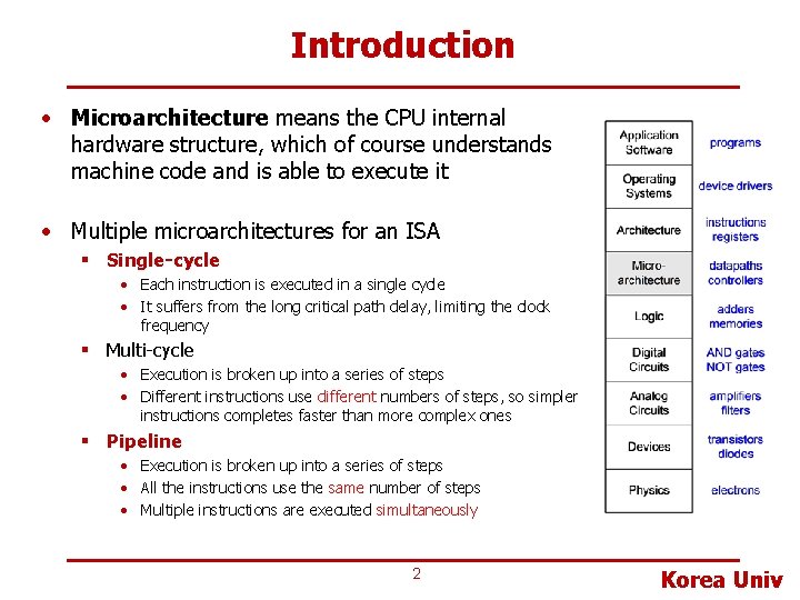
Introduction • Microarchitecture means the CPU internal hardware structure, which of course understands machine code and is able to execute it • Multiple microarchitectures for an ISA § Single-cycle • Each instruction is executed in a single cycle • It suffers from the long critical path delay, limiting the clock frequency § Multi-cycle • Execution is broken up into a series of steps • Different instructions use different numbers of steps, so simpler instructions completes faster than more complex ones § Pipeline • Execution is broken up into a series of steps • All the instructions use the same number of steps • Multiple instructions are executed simultaneously 2 Korea Univ

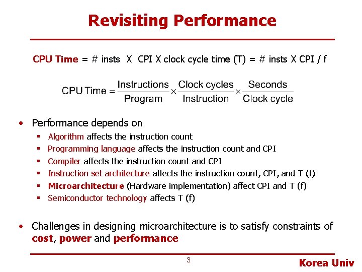
Revisiting Performance CPU Time = # insts X CPI X clock cycle time (T) = # insts X CPI / f • Performance depends on § § § Algorithm affects the instruction count Programming language affects the instruction count and CPI Compiler affects the instruction count and CPI Instruction set architecture affects the instruction count, CPI, and T (f) Microarchitecture (Hardware implementation) affect CPI and T (f) Semiconductor technology affects T (f) • Challenges in designing microarchitecture is to satisfy constraints of cost, power and performance 3 Korea Univ

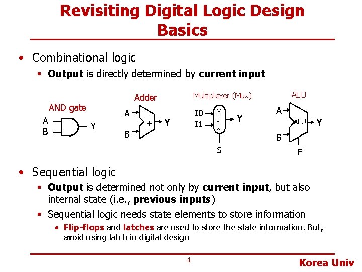
Revisiting Digital Logic Design Basics • Combinational logic § Output is directly determined by current input AND gate A B A Y + ALU Multiplexer (Mux) Adder I 0 I 1 Y B M u x S Y A ALU Y B F • Sequential logic § Output is determined not only by current input, but also internal state (i. e. , previous inputs) § Sequential logic needs state elements to store information • Flip-flops and latches are used to store the state information. But, avoid using latch in digital design 4 Korea Univ

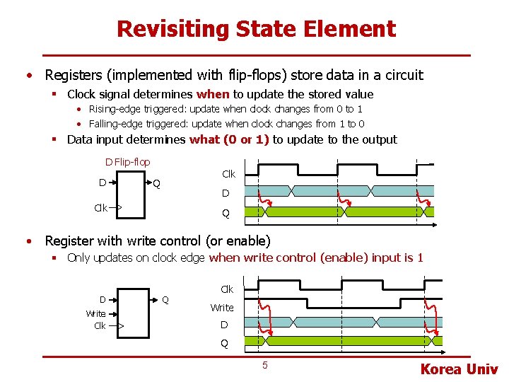
Revisiting State Element • Registers (implemented with flip-flops) store data in a circuit § Clock signal determines when to update the stored value • Rising-edge triggered: update when clock changes from 0 to 1 • Falling-edge triggered: update when clock changes from 1 to 0 § Data input determines what (0 or 1) to update to the output D Flip-flop D Clk Q • Register with write control (or enable) § Only updates on clock edge when write control (enable) input is 1 D Write Clk Q Clk Write D Q 5 Korea Univ

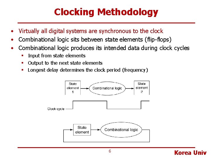
Clocking Methodology • Virtually all digital systems are synchronous to the clock • Combinational logic sits between state elements (flip-flops) • Combinational logic produces its intended data during clock cycles § Input from state elements § Output to the next state elements § Longest delay determines the clock period (frequency) 6 Korea Univ

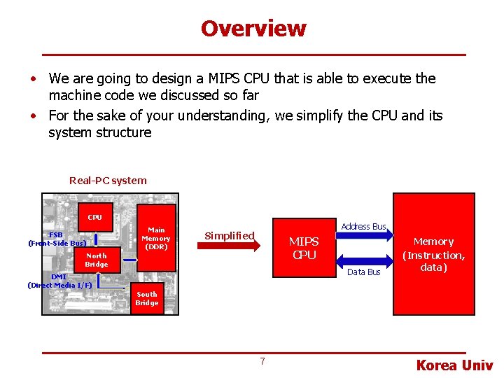
Overview • We are going to design a MIPS CPU that is able to execute the machine code we discussed so far • For the sake of your understanding, we simplify the CPU and its system structure Real-PC system CPU FSB (Front-Side Bus) Main Memory (DDR) Address Bus Simplified MIPS CPU North Bridge Data Bus DMI (Direct Media I/F) Memory (Instruction, data) South Bridge 7 Korea Univ

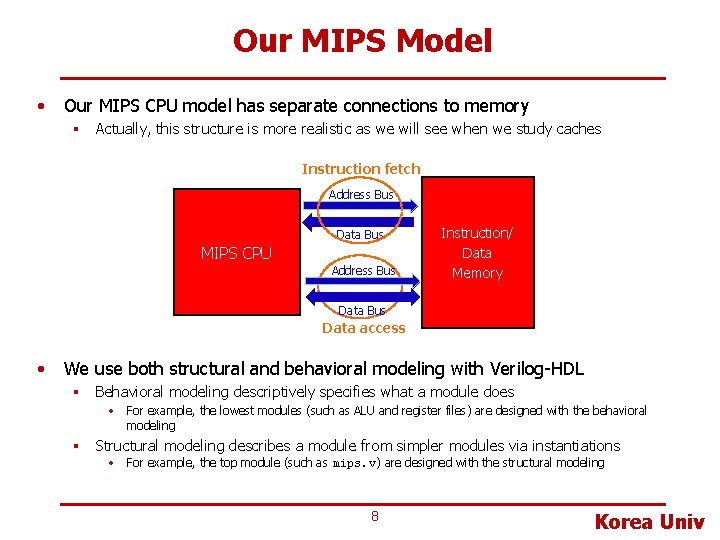
Our MIPS Model • Our MIPS CPU model has separate connections to memory § Actually, this structure is more realistic as we will see when we study caches Instruction fetch Address Bus Data Bus MIPS CPU Address Bus Instruction/ Data Memory Data Bus Data access • We use both structural and behavioral modeling with Verilog-HDL § Behavioral modeling descriptively specifies what a module does • For example, the lowest modules (such as ALU and register files) are designed with the behavioral modeling § Structural modeling describes a module from simpler modules via instantiations • For example, the top module (such as mips. v) are designed with the structural modeling 8 Korea Univ

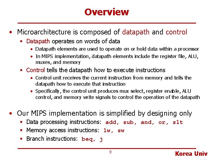
Overview • Microarchitecture is composed of datapath and control § Datapath operates on words of data • Datapath elements are used to operate on or hold data within a processor • In MIPS implementation, datapath elements include the register file, ALU, muxes, and memory § Control tells the datapath how to execute instructions • Control unit receives the current instruction from memory and tells the datapath how to execute that instruction • Specifically, the control unit produces mux select, register enable, ALU control, and memory write signals to control the operation of the datapath • Our MIPS implementation is simplified by designing only § Data processing instructions: add, sub, and, or, slt § Memory access instructions: lw, sw § Branch instructions: beq, j 9 Korea Univ

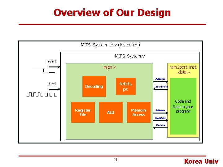
Overview of Our Design MIPS_System_tb. v (testbench) MIPS_System. v reset mips. v ram 2 port_inst _data. v Address clock fetch, pc Decoding Register File ALU Memory Access Instruction Address Code and Data in your program Data. Out Data. In 10 Korea Univ

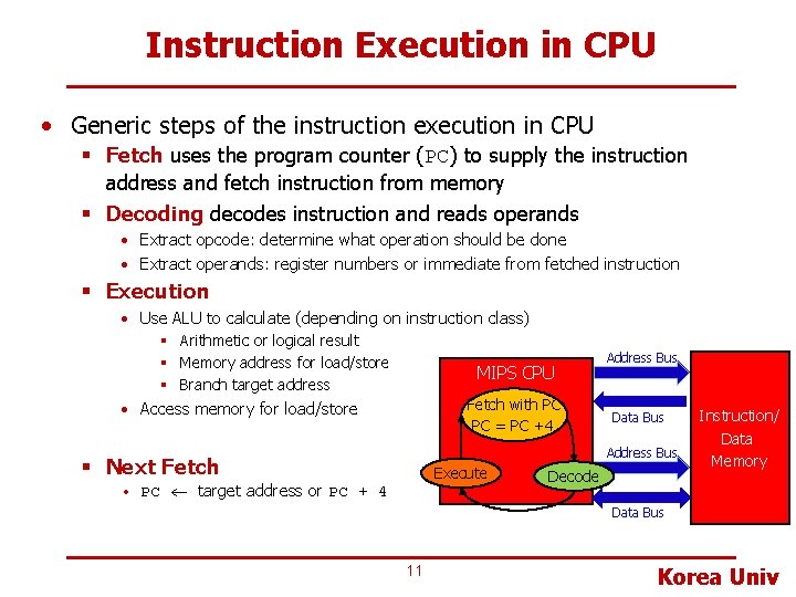
Instruction Execution in CPU • Generic steps of the instruction execution in CPU § Fetch uses the program counter (PC) to supply the instruction address and fetch instruction from memory § Decoding decodes instruction and reads operands • Extract opcode: determine what operation should be done • Extract operands: register numbers or immediate from fetched instruction § Execution • Use ALU to calculate (depending on instruction class) § Arithmetic or logical result § Memory address for load/store § Branch target address • Access memory for load/store MIPS CPU Fetch with PC PC = PC +4 Address Bus Data Bus Address Bus § Next Fetch Execute • PC target address or PC + 4 Decode Instruction/ Data Memory Data Bus 11 Korea Univ

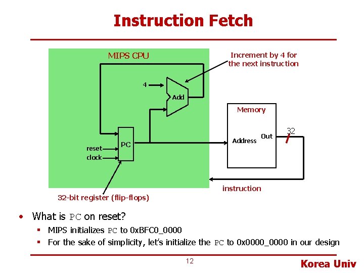
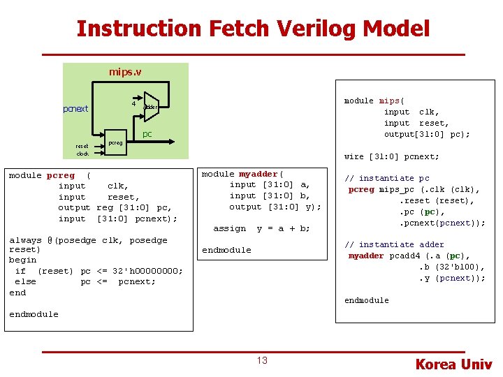
Instruction Fetch MIPS CPU Increment by 4 for the next instruction 4 Add Memory reset clock Address PC Out 32 instruction 32 -bit register (flip-flops) • What is PC on reset? § MIPS initializes PC to 0 x. BFC 0_0000 § For the sake of simplicity, let’s initialize the PC to 0 x 0000_0000 in our design 12 Korea Univ

Instruction Fetch Verilog Model mips. v 4 pcnext module mips( input clk, input reset, output[31: 0] pc); Adder pc reset clock pcreg module pcreg ( input clk, input reset, output reg [31: 0] pc, input [31: 0] pcnext); always @(posedge clk, posedge reset) begin if (reset) pc <= 32'h 0000; else pc <= pcnext; end wire [31: 0] pcnext; module myadder( input [31: 0] a, input [31: 0] b, output [31: 0] y); assign y = a + b; // instantiate pc pcreg mips_pc (. clk (clk), . reset (reset), . pc (pc), . pcnext(pcnext)); // instantiate adder myadder pcadd 4 (. a (pc), . b (32'b 100), . y (pcnext)); endmodule 13 Korea Univ

Memory • As studied in the Computer Logic Design, memory is classified into RAM (Random Access Memory) and ROM (Read-Only Memory) § RAM is classified into DRAM (Dynamic RAM) and SRAM (Static RAM) § DDR is a kind of DRAM • DDR is a short form of DDR (Double Data Rate) SDRAM (Synchronous DRAM) • DDR is used as main memory in modern computers • We use a Cyclone-II (Altera FPGA)-specific memory model because we port our design to the Cyclone-II FPGA 14 Korea Univ

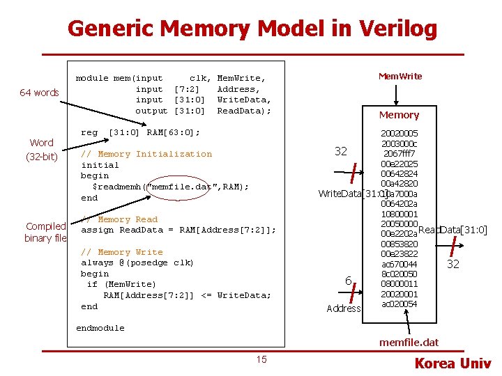
Generic Memory Model in Verilog 64 words Word (32 -bit) Compiled binary file module mem(input clk, input [7: 2] input [31: 0] output [31: 0] reg Mem. Write, Address, Write. Data, Read. Data); [31: 0] RAM[63: 0]; // Memory Initialization initial begin $readmemh("memfile. dat", RAM); end // Memory Read assign Read. Data = RAM[Address[7: 2]]; // Memory Write always @(posedge clk) begin if (Mem. Write) RAM[Address[7: 2]] <= Write. Data; end Memory 20020005 2003000 c 32 2067 fff 7 00 e 22025 00642824 00 a 42820 Write. Data[31: 0] 10 a 7000 a 0064202 a 10800001 20050000 00 e 2202 a Read. Data[31: 0] 00853820 00 e 23822 ac 670044 32 8 c 020050 6 08000011 20020001 ac 020054 Address endmodule memfile. dat 15 Korea Univ

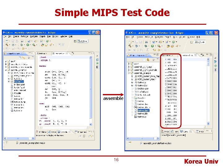
Simple MIPS Test Code assemble 16 Korea Univ

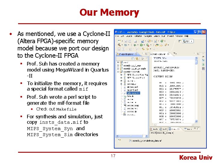
Our Memory • As mentioned, we use a Cyclone-II (Altera FPGA)-specific memory model because we port our design to the Cyclone-II FPGA § Prof. Suh has created a memory model using Mega. Wizard in Quartus -II § To initialize the memory, it requires a special format called mif § Prof. Suh wrote a perl script to generate the mif-format file • Check out Makefile § For synthesis and simulation, just copy insts_data. mif to MIPS_System_Syn and MIPS_System_Sim directories 17 Korea Univ

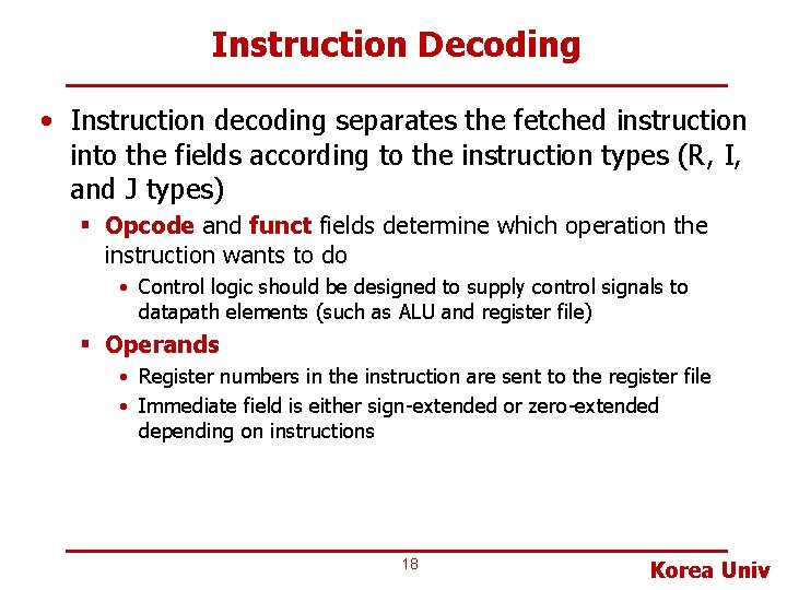
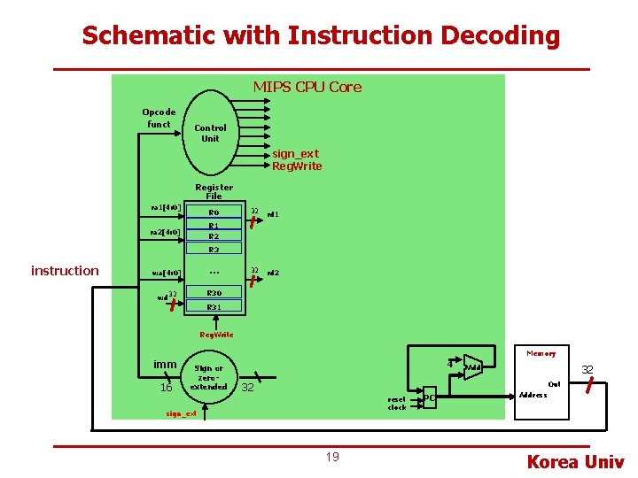
Instruction Decoding • Instruction decoding separates the fetched instruction into the fields according to the instruction types (R, I, and J types) § Opcode and funct fields determine which operation the instruction wants to do • Control logic should be designed to supply control signals to datapath elements (such as ALU and register file) § Operands • Register numbers in the instruction are sent to the register file • Immediate field is either sign-extended or zero-extended depending on instructions 18 Korea Univ

Schematic with Instruction Decoding MIPS CPU Core Opcode funct Control Unit sign_ext Reg. Write Register File ra 1[4: 0] R 0 32 rd 1 32 rd 2 R 1 R 2 ra 2[4: 0] R 3 instruction wa[4: 0] … wd 32 R 30 R 31 Reg. Write Memory imm 16 Sign or zeroextended 4 32 Add Out 32 reset clock sign_ext 19 PC Address Korea Univ
![Register File in Verilog module regfileinput 4 0 input 31 0 output 31 0 Register File in Verilog module regfile(input [4: 0] input [31: 0] output [31: 0]](https://slidetodoc.com/presentation_image_h/99220d135a9fa4cac0f41a7466da7b62/image-20.jpg)
Register File in Verilog module regfile(input [4: 0] input [31: 0] output [31: 0] clk, Reg. Write, ra 1, ra 2, wa, wd, rd 1, rd 2); 32 bits ra 1[4: 0] reg [31: 0] rf[31: 0]; // // Register File three ported register file read two ports combinationally write third port on rising edge of clock register 0 hardwired to 0 ra 2[4: 0] wa wd always @(posedge clk) if (Reg. Write) rf[wa] <= wd; 5 R 0 5 R 1 R 2 32 rd 1 R 3 5 … 32 R 30 32 rd 2 R 31 Reg. Write assign rd 1 = (ra 1 != 0) ? rf[ra 1] : 0; assign rd 2 = (ra 2 != 0) ? rf[ra 2] : 0; endmodule 20 Korea Univ

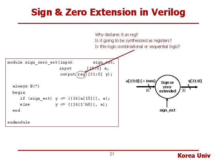
Sign & Zero Extension in Verilog Why declares it as reg? Is it going to be synthesized as registers? Is this logic combinational or sequential logic? module sign_zero_ext(input sign_ext, input [15: 0] a, output reg [31: 0] y); a[15: 0] (= imm) always @(*) begin if (sign_ext) y <= {{16{a[15]}}, a}; else y <= {{16{1'b 0}}, a}; end 16 Sign or zeroextended y[31: 0] 32 sign_ext endmodule 21 Korea Univ

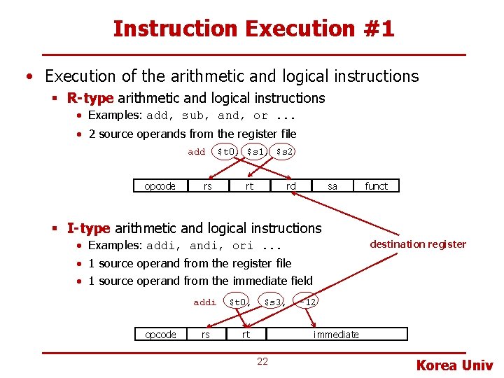
Instruction Execution #1 • Execution of the arithmetic and logical instructions § R-type arithmetic and logical instructions • Examples: add, sub, and, or. . . • 2 source operands from the register file add opcode rs $t 0, $s 1, $s 2 rt rd sa funct § I-type arithmetic and logical instructions • Examples: addi, andi, ori. . . destination register • 1 source operand from the register file • 1 source operand from the immediate field addi opcode rs $t 0, $s 3, -12 immediate rt 22 Korea Univ

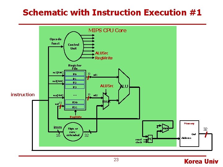
Schematic with Instruction Execution #1 MIPS CPU Core Opcode funct Control Unit ALUSrc Reg. Write Register File ra 1[4: 0] ra 2[4: 0] R 0 32 rd 1 R 2 ALUSrc R 3 instruction wa[4: 0] … wd 32 R 30 32 ALU rd 2 mux R 31 Reg. Write Memory imm 16 Sign or zeroextended 4 32 Add Out 32 reset clock 23 PC Address Korea Univ
![How to Design Mux in Verilog module mux 2 input 31 0 d 0 How to Design Mux in Verilog? module mux 2 (input [31: 0] d 0,](https://slidetodoc.com/presentation_image_h/99220d135a9fa4cac0f41a7466da7b62/image-24.jpg)
How to Design Mux in Verilog? module mux 2 (input [31: 0] d 0, input [31: 0] d 1, input s, output [31: 0] y); module mux 2 (input [31: 0] d 0, input [31: 0] d 1, input s, output reg [31: 0] always @(*) begin if (s) y <= d 1; else y <= d 0; endmodule OR assign y = s ? d 1 : d 0; endmodule Design it with parameter, so that this module can be used (instantiatiated) in any sized muxes in your design y); module datapath(………); wire [31: 0] writedata, signimm; wire [31: 0] srcb; wire alusrc module mux 2 #(parameter WIDTH = 8) (input [WIDTH-1: 0] d 0, d 1, input s, output [WIDTH-1: 0] y); assign y = s ? d 1 : d 0; endmodule // Instantiation mux 2 #(32) srcbmux(. d 0 (writedata), . d 1 (signimm), . s (alusrc), . y (srcb)); endmodule 24 Korea Univ

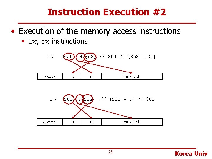
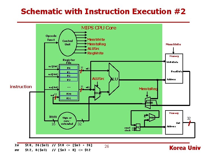
Instruction Execution #2 • Execution of the memory access instructions § lw, sw instructions lw opcode sw opcode $t 0, 24($s 3) // $t 0 <= [$s 3 + 24] rs rt $t 2, 8($s 3) rs immediate // [$s 3 + 8] <= $t 2 rt immediate 25 Korea Univ

Schematic with Instruction Execution #2 MIPS CPU Core Opcode funct Mem. Write Memto. Reg ALUSrc Reg. Write Control Unit Mem. Write Memory Register File ra 1[4: 0] ra 2[4: 0] R 0 Write. Data 32 rd 1 Read. Data R 1 R 2 ALUSrc R 3 instruction wa[4: 0] wd 32 … 32 ALU Address rd 2 Memto. Reg mux R 30 R 31 mux Memory imm 16 Sign or zeroextended 4 Out 32 reset clock lw sw $t 0, 24($s 3) // $t 0 <= [$s 3 + 24] $t 2, 8($s 3) // [$s 3 + 8] <= $t 2 32 Add 26 PC Address Korea Univ

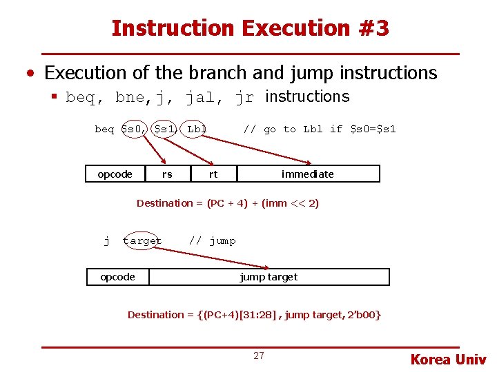
Instruction Execution #3 • Execution of the branch and jump instructions § beq, bne, j, jal, jr instructions beq $s 0, $s 1, Lbl opcode rs // go to Lbl if $s 0=$s 1 rt immediate Destination = (PC + 4) + (imm << 2) j target opcode // jump target Destination = {(PC+4)[31: 28] , jump target, 2’b 00} 27 Korea Univ

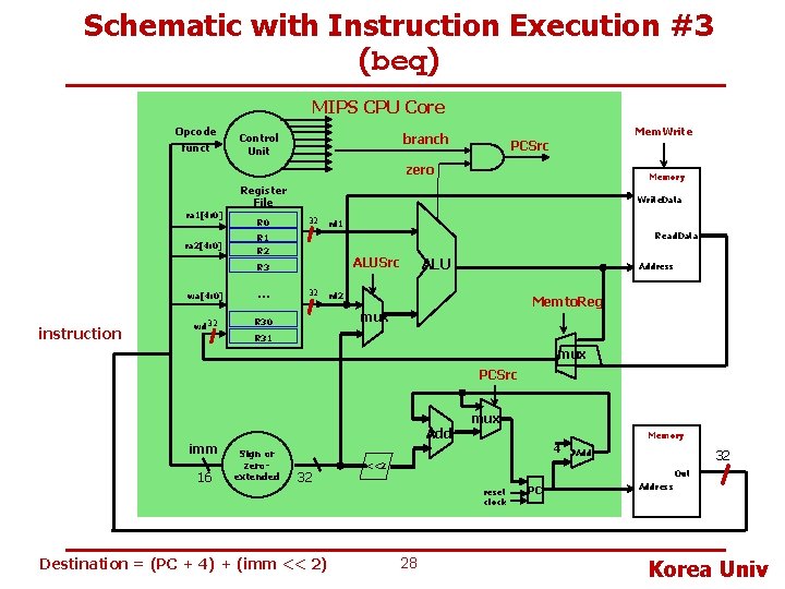
Schematic with Instruction Execution #3 (beq) MIPS CPU Core Opcode funct branch Control Unit Mem. Write PCSrc zero Memory Register File ra 1[4: 0] ra 2[4: 0] R 0 Write. Data 32 rd 1 Read. Data R 1 R 2 ALUSrc R 3 wa[4: 0] instruction wd 32 … 32 ALU Address rd 2 Memto. Reg mux R 30 R 31 mux PCSrc mux imm 16 Add Sign or zeroextended Memory 4 32 Out reset clock Destination = (PC + 4) + (imm << 2) 32 Add <<2 28 PC Address Korea Univ

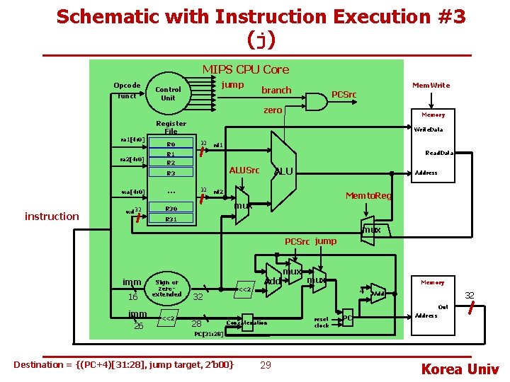
Schematic with Instruction Execution #3 (j) MIPS CPU Core Opcode funct jump Control Unit branch Mem. Write PCSrc zero Memory Register File ra 1[4: 0] ra 2[4: 0] R 0 Write. Data 32 rd 1 Read. Data R 1 R 2 ALUSrc R 3 wa[4: 0] instruction wd 32 … 32 ALU Address rd 2 Memto. Reg mux R 30 R 31 mux PCSrc jump mux imm 16 imm 26 Sign or zeroextended <<2 32 Add mux Memory 4 32 Add Out <<2 28 Concatenation reset clock PC Address PC[31: 28] Destination = {(PC+4)[31: 28], jump target, 2’b 00} 29 Korea Univ

Demo • Synthesis with Quartus-II • Simulation with Model. Sim 30 Korea Univ

Backup Slides 31 Korea Univ

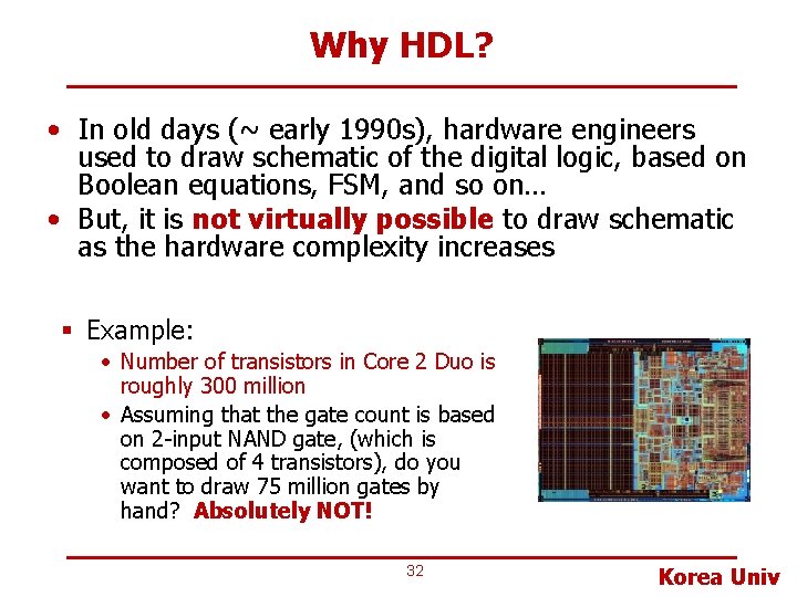
Why HDL? • In old days (~ early 1990 s), hardware engineers used to draw schematic of the digital logic, based on Boolean equations, FSM, and so on… • But, it is not virtually possible to draw schematic as the hardware complexity increases § Example: • Number of transistors in Core 2 Duo is roughly 300 million • Assuming that the gate count is based on 2 -input NAND gate, (which is composed of 4 transistors), do you want to draw 75 million gates by hand? Absolutely NOT! 32 Korea Univ

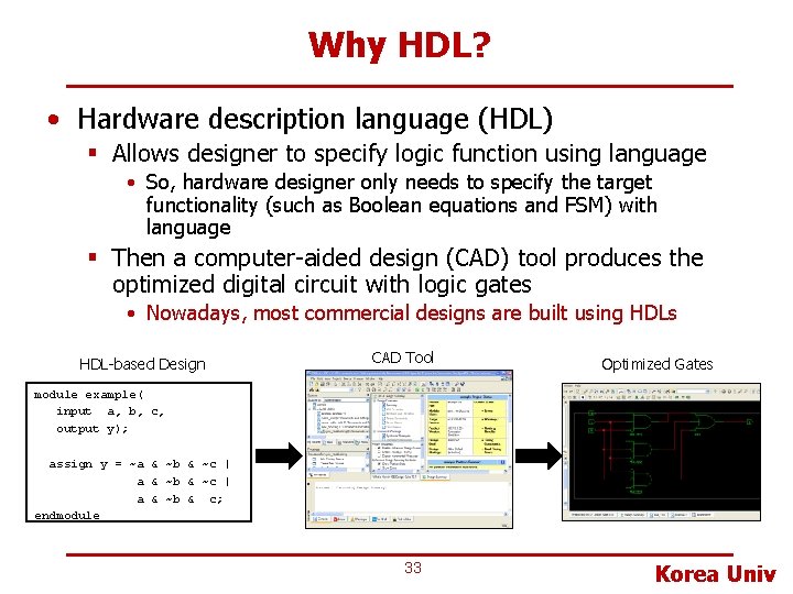
Why HDL? • Hardware description language (HDL) § Allows designer to specify logic function using language • So, hardware designer only needs to specify the target functionality (such as Boolean equations and FSM) with language § Then a computer-aided design (CAD) tool produces the optimized digital circuit with logic gates • Nowadays, most commercial designs are built using HDLs HDL-based Design CAD Tool Optimized Gates module example( input a, b, c, output y); assign y = ~a & ~b & ~c | a & ~b & c; endmodule 33 Korea Univ

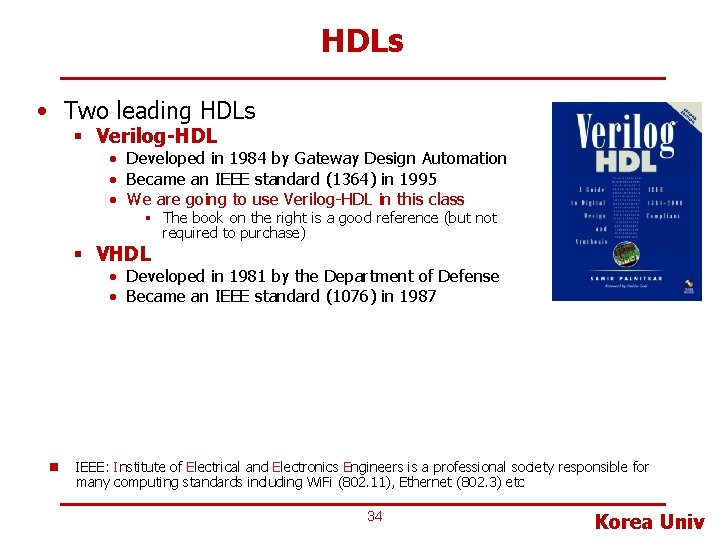
HDLs • Two leading HDLs § Verilog-HDL • Developed in 1984 by Gateway Design Automation • Became an IEEE standard (1364) in 1995 • We are going to use Verilog-HDL in this class § The book on the right is a good reference (but not required to purchase) § VHDL • Developed in 1981 by the Department of Defense • Became an IEEE standard (1076) in 1987 n IEEE: Institute of Electrical and Electronics Engineers is a professional society responsible for many computing standards including Wi. Fi (802. 11), Ethernet (802. 3) etc 34 Korea Univ

HDL to (Logic) Gates • There are 3 steps to design hardware with HDL 1. Hardware design with HDL • Describe your hardware with HDL § When describing circuits using an HDL, it’s critical to think of the hardware the code should produce 2. Simulation • Once you design your hardware with HDL, you need to verify if the design is implemented correctly § § § Input values are applied to your design with HDL Outputs checked for correctness Millions of dollars saved by debugging in simulation instead of hardware 3. Synthesis • Transforms HDL code into a netlist, describing the hardware § Netlist is a text file describing a list of logic gates and the wires connecting them 35 Korea Univ

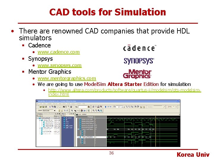
CAD tools for Simulation • There are renowned CAD companies that provide HDL simulators § Cadence • www. cadence. com § Synopsys • www. synopsys. com § Mentor Graphics • www. mentorgraphics. com • We are going to use Model. Sim Altera Starter Edition for simulation • http: //www. altera. com/products/software/quartus-ii/modelsim/qts-modelsimindex. html 36 Korea Univ

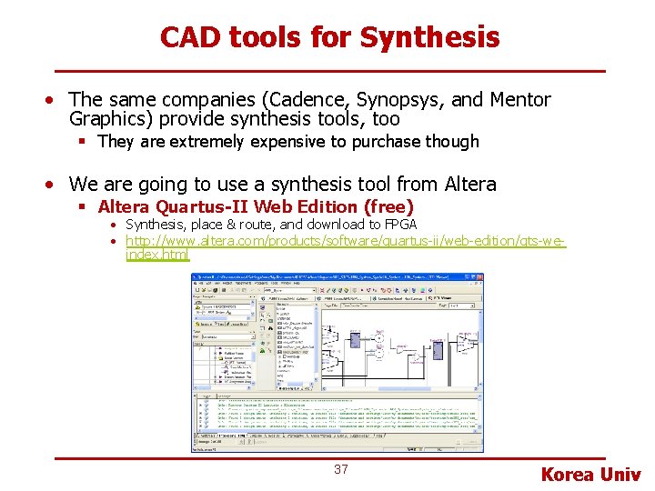
CAD tools for Synthesis • The same companies (Cadence, Synopsys, and Mentor Graphics) provide synthesis tools, too § They are extremely expensive to purchase though • We are going to use a synthesis tool from Altera § Altera Quartus-II Web Edition (free) • Synthesis, place & route, and download to FPGA • http: //www. altera. com/products/software/quartus-ii/web-edition/qts-weindex. html 37 Korea Univ

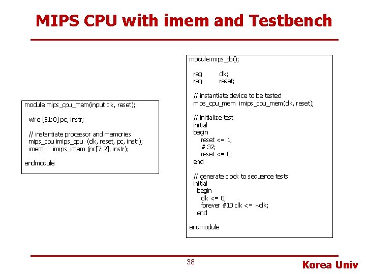
MIPS CPU with imem and Testbench module mips_tb(); reg module mips_cpu_mem(input clk, reset); wire [31: 0] pc, instr; // instantiate processor and memories mips_cpu imips_cpu (clk, reset, pc, instr); imem imips_imem (pc[7: 2], instr); endmodule clk; reset; // instantiate device to be tested mips_cpu_mem imips_cpu_mem(clk, reset); // initialize test initial begin reset <= 1; # 32; reset <= 0; end // generate clock to sequence tests initial begin clk <= 0; forever #10 clk <= ~clk; endmodule 38 Korea Univ