Computing with Leakage Currents Nikhil Jayakumar Kanupriya Gulati




- Slides: 25

Computing with Leakage Currents Nikhil Jayakumar, Kanupriya Gulati, Rajesh Garg and Sunil P. Khatri ECE Department Texas A&M University 1

Outline § Sub-threshold circuits – the opportunity § Challenges § Process/temperature/voltage variations § Energy minimization in sub-threshold circuits § Re-claiming the speed penalty § What’s next? 2

Introduction § Power consumption has become a significant hurdle for recent ICs § Higher power consumption leads to § Shorter battery life § Higher on-chip temperatures – reduced operating life of the chip § There is a large and growing class of applications where power reduction is paramount – not speed. § Such applications are ideal candidates for subthreshold circuit design. § OK, so what is sub-threshold design? ? 3

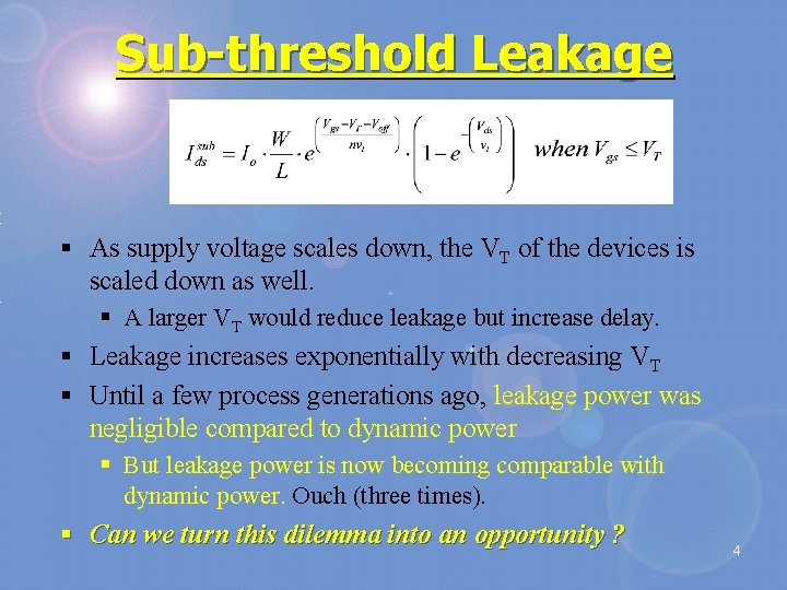
Sub-threshold Leakage § As supply voltage scales down, the VT of the devices is scaled down as well. § A larger VT would reduce leakage but increase delay. § Leakage increases exponentially with decreasing VT § Until a few process generations ago, leakage power was negligible compared to dynamic power § But leakage power is now becoming comparable with dynamic power. Ouch (three times). § Can we turn this dilemma into an opportunity ? 4

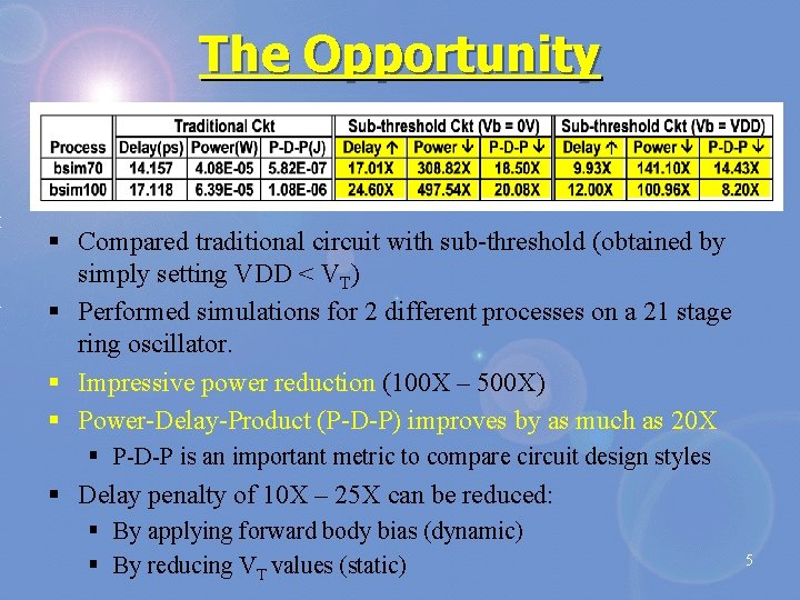
The Opportunity § Compared traditional circuit with sub-threshold (obtained by simply setting VDD < VT) § Performed simulations for 2 different processes on a 21 stage ring oscillator. § Impressive power reduction (100 X – 500 X) § Power-Delay-Product (P-D-P) improves by as much as 20 X § P-D-P is an important metric to compare circuit design styles § Delay penalty of 10 X – 25 X can be reduced: § By applying forward body bias (dynamic) § By reducing VT values (static) 5

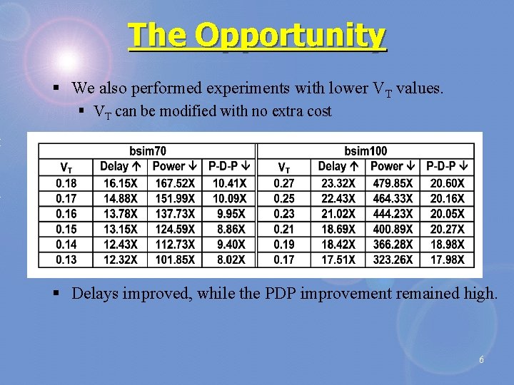
The Opportunity § We also performed experiments with lower VT values. § VT can be modified with no extra cost § Delays improved, while the PDP improvement remained high. 6

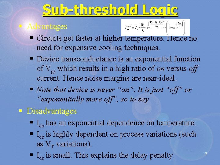
Sub-threshold Logic § Advantages § Circuits get faster at higher temperature. Hence no need for expensive cooling techniques. § Device transconductance is an exponential function of Vgs which results in a high ratio of on versus off current. Hence noise margins are near-ideal. § Note that device is never “on”. It is just “off” or “exponentially more off”, so to say § Disadvantages § Ids has an exponential dependence on temperature. § Ids is highly dependent on process variations (such as VT variations). § Ids is small. This explains the delay penalty 7

Solving the Problem of Delay Sensitivity to Process, Voltage and Temperature Variations 8

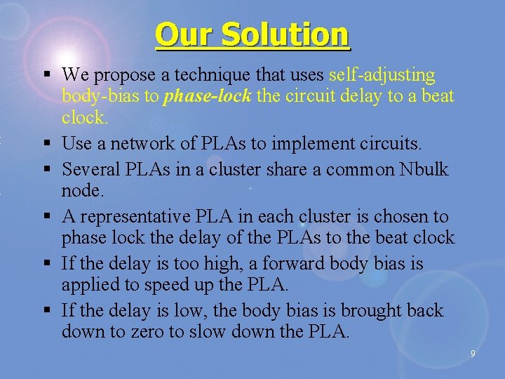
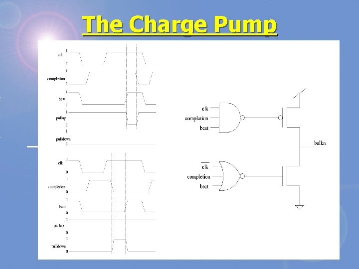
Our Solution § We propose a technique that uses self-adjusting body-bias to phase-lock the circuit delay to a beat clock. § Use a network of PLAs to implement circuits. § Several PLAs in a cluster share a common Nbulk node. § A representative PLA in each cluster is chosen to phase lock the delay of the PLAs to the beat clock § If the delay is too high, a forward body bias is applied to speed up the PLA. § If the delay is low, the body bias is brought back down to zero to slow down the PLA. 9

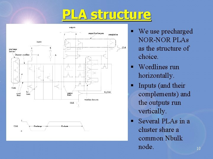
PLA structure § We use precharged NOR-NOR PLAs as the structure of choice. § Wordlines run horizontally. § Inputs (and their complements) and the outputs run vertically. § Several PLAs in a cluster share a common Nbulk node. 10

The Charge Pump 11

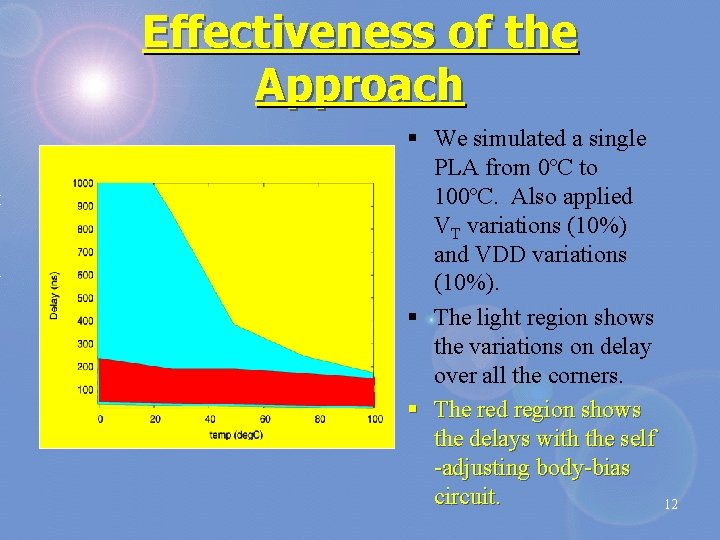
Effectiveness of the Approach § We simulated a single PLA from 0ºC to 100ºC. Also applied VT variations (10%) and VDD variations (10%). § The light region shows the variations on delay over all the corners. § The red region shows the delays with the self -adjusting body-bias circuit. 12

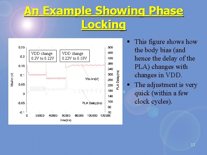
An Example Showing Phase Locking VDD change 0. 2 V to 0. 22 V VDD change 0. 22 V to 0. 18 V § This figure shows how the body bias (and hence the delay of the PLA) changes with changes in VDD. § The adjustment is very quick (within a few clock cycles). 13

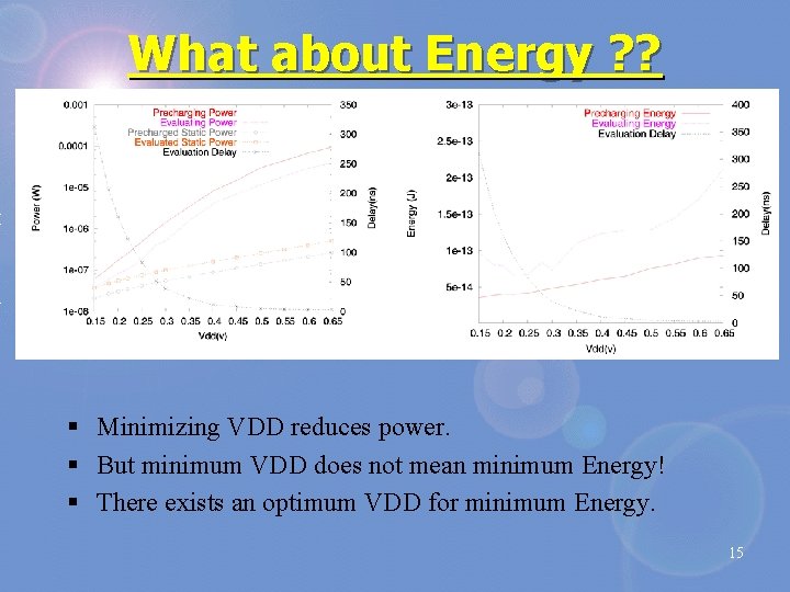
What about Energy Minimization Minimum Power does not mean Minimum Energy… We are interested in mimimum energy operation given the application scenario envisioned 14

What about Energy ? ? § Minimizing VDD reduces power. § But minimum VDD does not mean minimum Energy! § There exists an optimum VDD for minimum Energy. 15

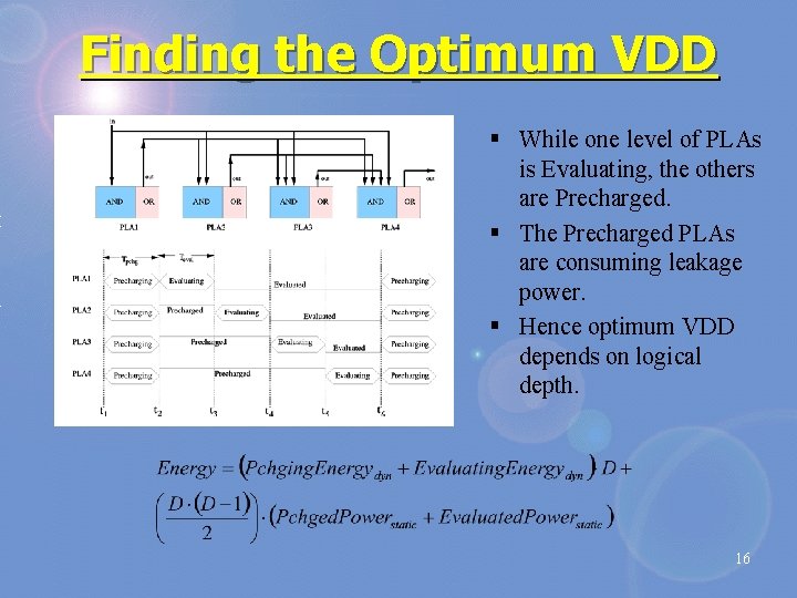
Finding the Optimum VDD § While one level of PLAs is Evaluating, the others are Precharged. § The Precharged PLAs are consuming leakage power. § Hence optimum VDD depends on logical depth. 16

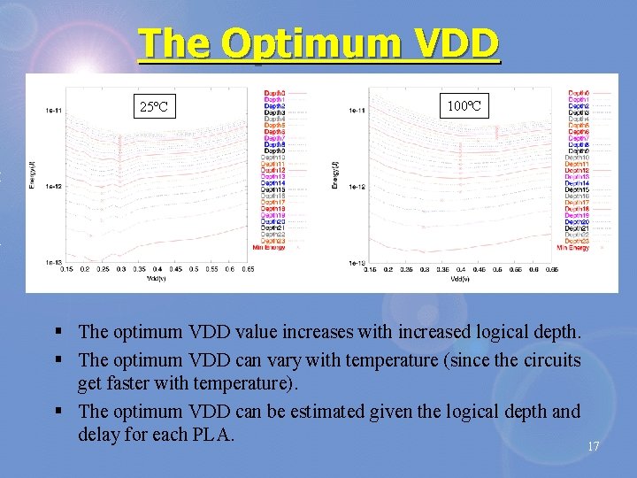
The Optimum VDD 25ºC 100ºC § The optimum VDD value increases with increased logical depth. § The optimum VDD can vary with temperature (since the circuits get faster with temperature). § The optimum VDD can be estimated given the logical depth and delay for each PLA. 17

Reclaiming Part of the Speed Penalty 18

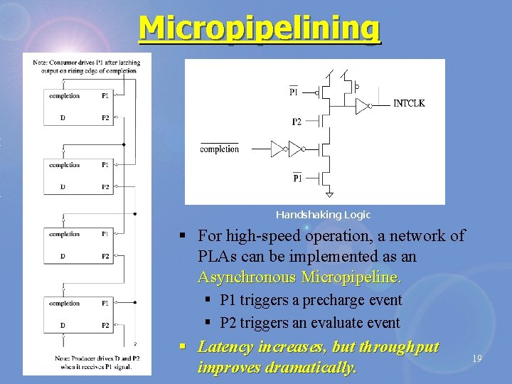
Micropipelining Handshaking Logic § For high-speed operation, a network of PLAs can be implemented as an Asynchronous Micropipeline. § P 1 triggers a precharge event § P 2 triggers an evaluate event § Latency increases, but throughput improves dramatically. 19

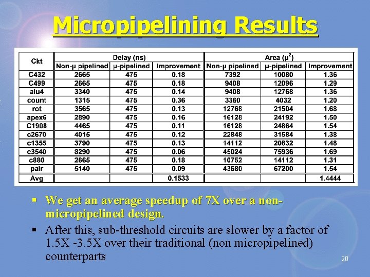
Micropipelining Results § We get an average speedup of 7 X over a nonmicropipelined design. § After this, sub-threshold circuits are slower by a factor of 1. 5 X -3. 5 X over their traditional (non micropipelined) counterparts 20

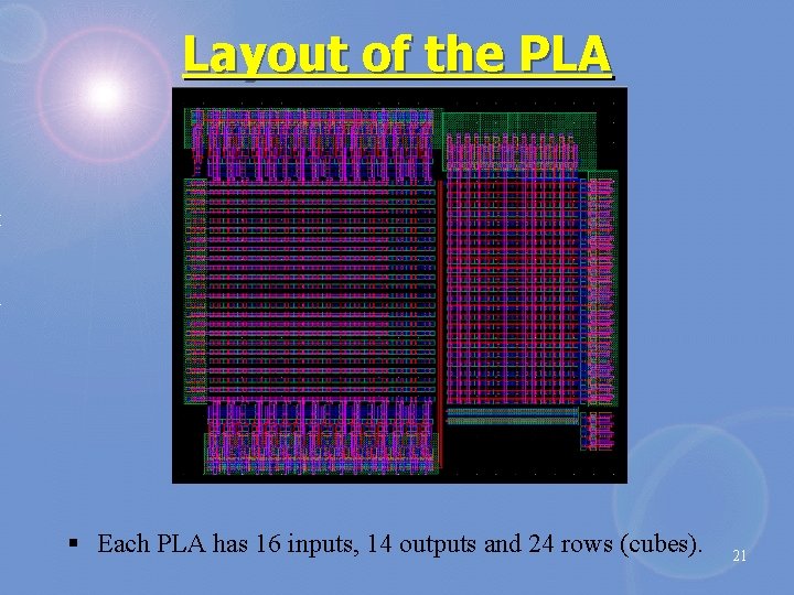
Layout of the PLA § Each PLA has 16 inputs, 14 outputs and 24 rows (cubes). 21

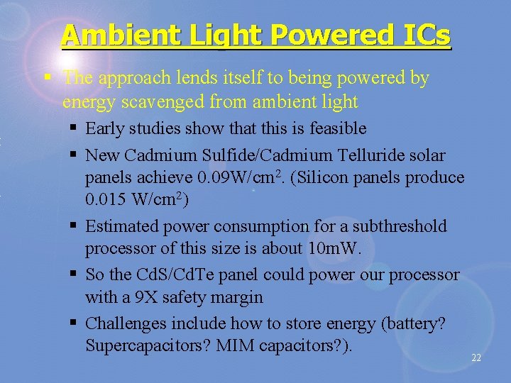
Ambient Light Powered ICs § The approach lends itself to being powered by energy scavenged from ambient light § Early studies show that this is feasible § New Cadmium Sulfide/Cadmium Telluride solar panels achieve 0. 09 W/cm 2. (Silicon panels produce 0. 015 W/cm 2) § Estimated power consumption for a subthreshold processor of this size is about 10 m. W. § So the Cd. S/Cd. Te panel could power our processor with a 9 X safety margin § Challenges include how to store energy (battery? Supercapacitors? MIM capacitors? ). 22

What next? § Explore extensions to structured ASIC approaches § Fabrication of a subthreshold design (in 2006) § Mixed-signal – with small processor and transceiver on a single die. § Set up a small hardware lab for debug/diagnosis § Validate the experiments we discussed § Hope to use this test-chip to validate other ideas as well. § Develop a design methodology for subthreshold electronics, tuned for widespread use. 23

Summary § Sub-threshold circuit design is promising due to extreme low power. § The delay phase locking approach helps sub-threshold logic design overcome the hurdle of sensitivity to PVT variations. § This can help achieve a significant yield improvement. § The study on optimum VDD for minimum Energy helps to fix an optimum VDD for a given logical depth. § Micro-pipelining helps bridge the delay gap. § Sub-threshold design approaches are appealing for a widening class of low power or energy applications. § Goal : Help bring sub-threshold logic design into the 24 mainstream of VLSI technology.

Thank you!! 25