Fabrication and characterization of Schottky MOSFETs Two mask

金屬氧化物半導體場效電晶體之製作 Fabrication and characterization of Schottky MOSFETs Two mask process

MOSFET �N-channel MOSFET, n. FET
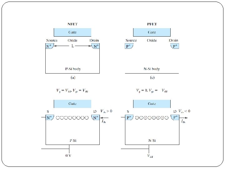

本實驗所做之元件 利用Schottky barrier阻擋body to drain漏 電 p. FET n. FET

MOS: Gate Voltage Eq.

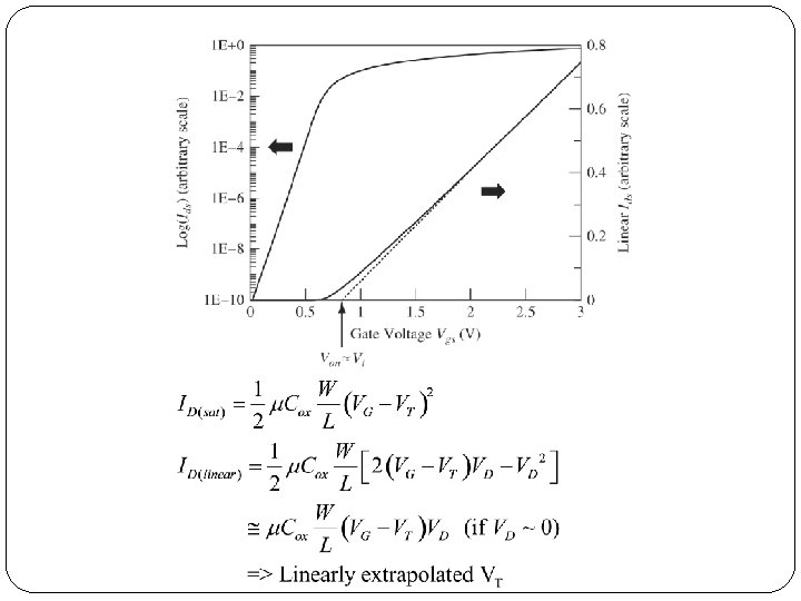
Strong Inversion �The electron concentration at the surface equals the hole concentration in the bulk Si.
")
Subthreshold (VG<VT)
 �The gate control is degraded by the penetration of drain")
Short Channel Effects (SCE) �The gate control is degraded by the penetration of drain electric field in short-channel devices.
 �The barrier is lowered in short-channel devices.")
Short Channel Effects (SCE) �The barrier is lowered in short-channel devices.
 �VT of short channel devices is lower than that of")
Short Channel Effects (SCE) �VT of short channel devices is lower than that of long channel devices. VT roll-off
 �")
Drain-Induced Barrier Lowering (DIBL) �
")
Drain-Induced Barrier Lowering (DIBL)
 �Off-state (VG<0 for n. FET) �Band-to-band tunneling")
Gate-Induced Drain Leakage (GIDL) �Off-state (VG<0 for n. FET) �Band-to-band tunneling
 Equivalent oxide thickness (EOT)")
Inversion Layer Thickness Capacitance equivalent thickness (CET) Equivalent oxide thickness (EOT)

The goal of this class is to make a Schottky MOSFETs Gate Source Drain Source Si. O 2 Metal Cross section Top view Gate Metal Si. O 2 Si Drain Metal Si. O 2
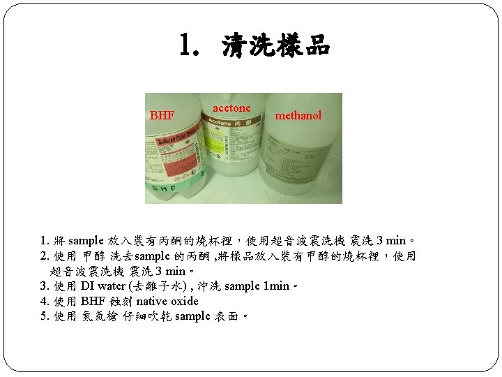

2. 成長氧化層 星期一班 四片 Si. O 2 PECVD+900 o. C FGA anneal 1 min 兩片ntype兩片type 星期二班 四片 Si. O 2乾氧 0. 5 h 兩片ntype兩片type

數據處理 1. Id-Vg & Id-Vd 2. Vt、on/off、SS、DIBL 3. What is GIDL (Gate Induced Drain Leakage)
 �How does a Schottky MOSFET work? �How to achieve 1 -mask")
結報問題 (4/29, 30) �How does a Schottky MOSFET work? �How to achieve 1 -mask process? Please draw the process flow. �Compare and discuss the pros and cons of 1 -mask process and 2 -mask process of MOSFETs. �What are the advantages of Fin. FETs as compared to planar MOSFETs?
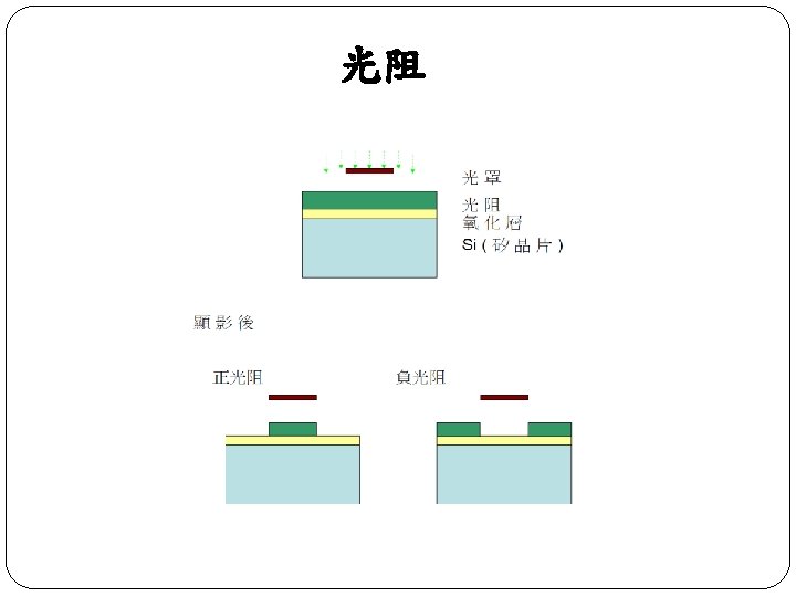
 �Loop up for the MSDS information of photoresist (AZ 5214 E) and")
結報問題 (5/6) �Loop up for the MSDS information of photoresist (AZ 5214 E) and developer (300 MIF). �Please explain the difference between positive photoresist and negative photoresist. �What are the purposes of soft bake and hard bake? �Please look up for the evolution of lithography technology.
 �What is alignment mark and its purpose? �Please define the active region")
結報問題 (5/13) �What is alignment mark and its purpose? �Please define the active region (channel) using our 2 - mask process. �The etching of oxide on S/D is required for S/D opening. Please compare the methods of reactive-ion etching (RIE) and wet etching (BOE). �Do our MOSFETs have gate-to-source/drain overlap or underlap? What are the effects of gate-tosource/drain overlap or underlap on MOSFETs?
 �Explain DIBL, and show DIBL in our IV curves. �Explain GIDL,")
結報問題 (5/20, 21) �Explain DIBL, and show DIBL in our IV curves. �Explain GIDL, and show GIDL in our IV curves. �What are the differences and purposes of the two oxide layers in our 2 -mask MOSFETs?
- Slides: 27