Amplifiers From Ideal to Real Why amplify Gain


 amplifier www. corollarytheorems. com/Design/opamp. htm A non-linear amplifier used to emphasis positive")

 d. B = 20*log 10(out/in) (Implies first order LP")

 • transformer isolation")


- Slides: 21
Amplifiers: From Ideal to Real • Why amplify? • Gain = Vout / Vin = sensitivity • Ideal Op Amp • Negative gain summation amplifier • Positive gain for increased Rin • Differential amplifier circuit • Gain-bandwidth product; CMRR • Nonlinear gain: The ideal diode • Instrumentation Amp • Isolation Amplifier
References: • Horowitz & Hill, The Art of Electronics, Cambridge Univ Press • James K. Roberge, Operational Amplifiers: Theory & Practice can download at: http: //web. mit. edu/klund/www/books/opamps 181. pdf • Burr-Brown HANDBOOK OF OPERATIONAL AMPLIFIER APPLICATIONS can download at: http: //focus. ti. com/lit/an/sboa 092 a. pdf
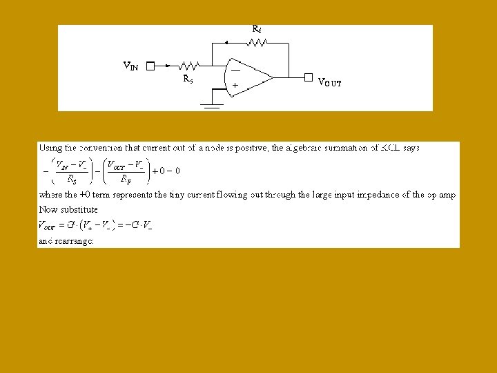
If Rf = 1000*Rs and G is 106, then Vin is in the range of 1 m. V, a so-called virtual ground.
Summation
Input impedance of NGSA • Input resistance = Vin/Iin = R 1= Rs ≈ 1 KΩ • Way less than the 1012Ω of the op amp itself • NG: R 1 may become voltage divider with sensor output resistance • Impedance includes frequency-dependent current-voltage relationship e. g. V(jω)=jωC*I(jω); impedance is a complex number mechatronics. mech. northwestern. edu/design_ref/electrical_design
Unity Gain Voltage Follower A good circuit for isolation http: //ytdp. ee. wits. ac. za/cctpng/Follower. png
Positive gain single input op amp ckt If Rs = 0 then Vout = Vin, UGVF The positive gain amplifier cannot have a gain less than 1. It can have only one input.
Differential amplifier with external resistors
Current-voltage relationship of a diode • Where k. T/q is about 25 m. V at room temp http: //keywon. com/wiki/images/ http: //electricalandelectronics. org
Ideal diode / half wave rectifer • When VIN > 0 volts output current can flow through the diode and does so until Vin = Vout. (low Rf, like UGVF) • When Vin < 0 the diode looks like a high resistance, the op amp output saturates at the negative supply voltage, and the left resistor "pulls down" VOUT until it's zero.
Log amplifier http: //www. regentsprep. org/Regents/math/algtrig/ ATP 8 b/exponential. Function. htm
Absolute value / Full wave rectifier www. eleinmec. com/ www. physics. udel. edu/~nowak/phys 645/More_opamp_circuits. htm
A compression function of input: suppresses large spikes on input
Exponential (anti-log) amplifier www. corollarytheorems. com/Design/opamp. htm A non-linear amplifier used to emphasis positive spikes in waveform; makes sense only when Vs > 0. … getting the signs of Vin and Vout figured out…
Op Amp as integrator Where we know a capacitor’s current-voltage relationship is (from Laplace transforms)
GBWP and CMRR (LF 353) d. B = 20*log 10(out/in) (Implies first order LP filter in op amp)
Instrumentation Amplifier AD 524 • No external components needed • pins to select gains of 10, 1000. • GBWP 25 MHz • Common mode rejection ratio of 120 d. B • Data sheet: www. analog. com/static/imported-files/data_sheets/AD 524. pdf • p. 4: differential resistance 109Ω • p. 8: Absolute Maximum Ratings dimensions in mm • p. 10: CMRR (freq) Gain (freq) • Settling time: 10μsec • p. 18: Ground, analog and digital; ground mecca • www. analog. com/en/other-products/militaryaerospace/ad 524/products/product. html#ppa_print_table
Isolation Amplifier AD 203 • UGVF • optical isolation; (wireless isolation) • transformer isolation • www. analog. com/en/amplifiers-and-comparators/isolationamplifiers/ad 203/products/product. html • Data sheet: www. analog. com/static/imported-files/data_sheets/AD 203 SN. pdf • Modulator is a Volt→Freq converter on input, and “tach” on output • single +15 v supply • input impedance 1012Ω • low GBWP about 1 MHz • CMRR about 120 d. B
Iso Amp block diagram
Op amp as example of negative feedback • When we come later to the topic of automatic control by negative feedback, we will see the op amp as a good example