A 190 210 GHz Power Amplifier with 17
![250 nm In. P HBT Process (Teledyne [6]) • • Mm-wave amplifier requires fast 250 nm In. P HBT Process (Teledyne [6]) • • Mm-wave amplifier requires fast](https://slidetodoc.com/presentation_image_h2/9a864fe23005c5b9d1c50b00c56c598e/image-6.jpg)

![References [1] M. J. W. Rodwell et al. , “ 100 -340 GHz Systems: References [1] M. J. W. Rodwell et al. , “ 100 -340 GHz Systems:](https://slidetodoc.com/presentation_image_h2/9a864fe23005c5b9d1c50b00c56c598e/image-23.jpg)
- Slides: 26

A 190 -210 GHz Power Amplifier with 17. 718. 5 d. Bm Output Power and 6. 9 -8. 5% PAE A. Ahmed 1, 2, U. Soylu 2, M. Seo 3, M. Urteaga 4, J. Buckwalter 2, and M. Rodwell 2 1 Marki Microwave Inc. , CA 2 ECE, University of California, Santa Barbara, USA 3 ECE, Sungkyunkwan University, South Korea 4 Teledyne Scientific Company, Thousand Oaks, CA, USA Th 02 C. 2

Outline • Motivation for mm-wave frequencies and prior work. • Application for the amplifier. • Amplifier design – Power and driver cells – Low-loss compact combiner • Measurement results • Summary and conclusion Th 02 C. 2 2

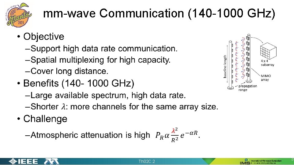
mm-wave Communication (140 -1000 GHz) • Th 02 C. 2 3

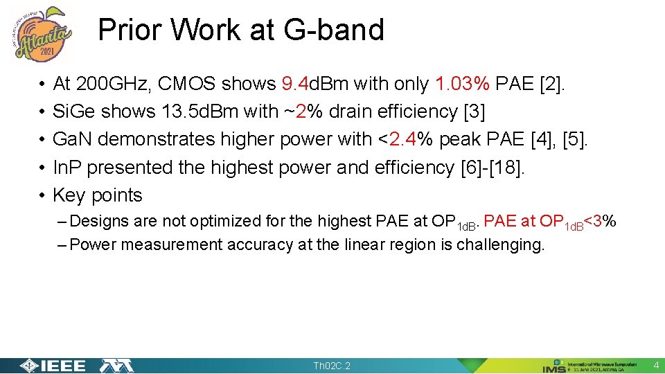
Prior Work at G-band • • • At 200 GHz, CMOS shows 9. 4 d. Bm with only 1. 03% PAE [2]. Si. Ge shows 13. 5 d. Bm with ~2% drain efficiency [3] Ga. N demonstrates higher power with <2. 4% peak PAE [4], [5]. In. P presented the highest power and efficiency [6]-[18]. Key points – Designs are not optimized for the highest PAE at OP 1 d. B<3% – Power measurement accuracy at the linear region is challenging. Th 02 C. 2 4

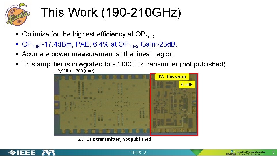
This Work (190 -210 GHz) • • Optimize for the highest efficiency at OP 1 d. B~17. 4 d. Bm, PAE: 6. 4% at OP 1 d. B, Gain~23 d. B. Accurate power measurement at the linear region. This amplifier is integrated to a 200 GHz transmitter (not published). 2, 900 x 1, 200 (um 2) PA this work 4 cells 200 GHz transmitter, not published Th 02 C. 2 5
![250 nm In P HBT Process Teledyne 6 Mmwave amplifier requires fast 250 nm In. P HBT Process (Teledyne [6]) • • Mm-wave amplifier requires fast](https://slidetodoc.com/presentation_image_h2/9a864fe23005c5b9d1c50b00c56c598e/image-6.jpg)
250 nm In. P HBT Process (Teledyne [6]) • • Mm-wave amplifier requires fast technologies. fmax=650 GHz. BVCEo=4. 5 V. Jmax=3 m. A/µm. Four Au interconnect. MIM cap (0. 3 f. F/µm 2). TFR (50Ω/square). Cross section of TSC 250 IC Th 02 C. 2 6

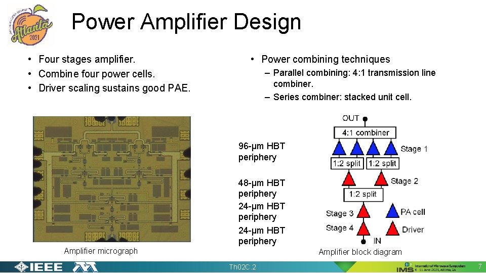
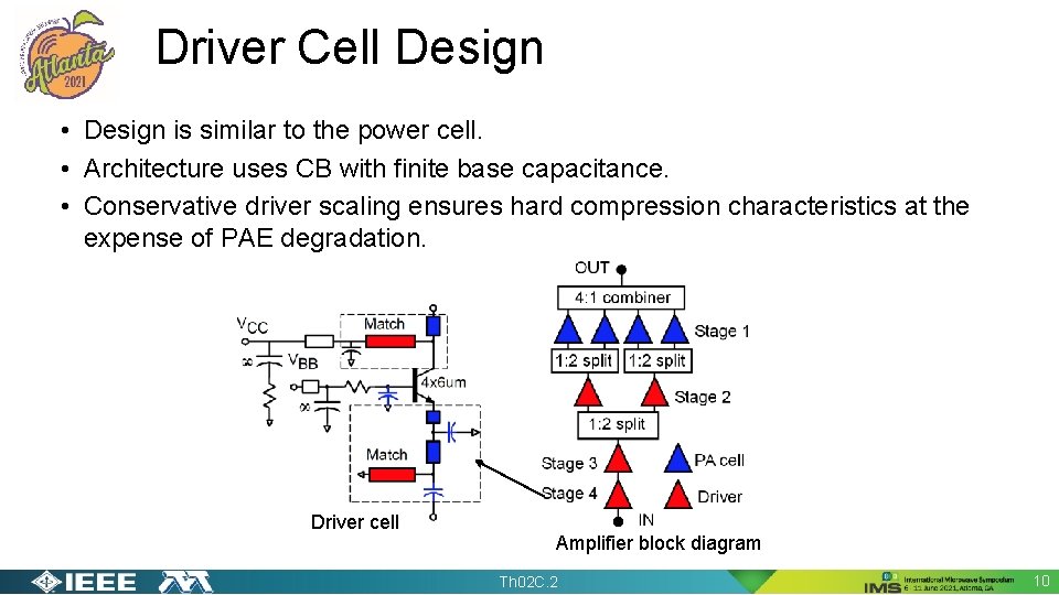
Power Amplifier Design • Four stages amplifier. • Combine four power cells. • Driver scaling sustains good PAE. • Power combining techniques – Parallel combining: 4: 1 transmission line combiner. – Series combiner: stacked unit cell. 96 -μm HBT periphery 48 -μm HBT periphery 24 -μm HBT periphery Amplifier micrograph Amplifier block diagram Th 02 C. 2 7

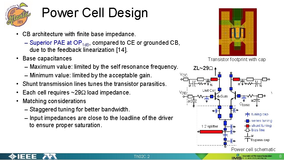
Power Cell Design • CB architecture with finite base impedance. – Superior PAE at OP 1 d. B, compared to CE or grounded CB, due to the feedback linearization [14]. • Base capacitances – Maximum value: limited by the self resonance frequency. – Minimum value: limited by the acceptable gain. • Shunt transmission lines tunes the transistor parasitics. • Each cell requires ~29 W load impedance. • Matching considerations – Staggered tuning for better bandwidth. – Input impedances are close to the loadline of the driver to ensure proper saturation. Transistor footprint with cap ZL~29 W Power cell schematic Th 02 C. 2 8

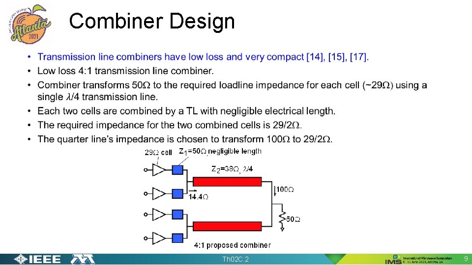
Combiner Design • Th 02 C. 2 9

Driver Cell Design • Design is similar to the power cell. • Architecture uses CB with finite base capacitance. • Conservative driver scaling ensures hard compression characteristics at the expense of PAE degradation. Driver cell Amplifier block diagram Th 02 C. 2 10

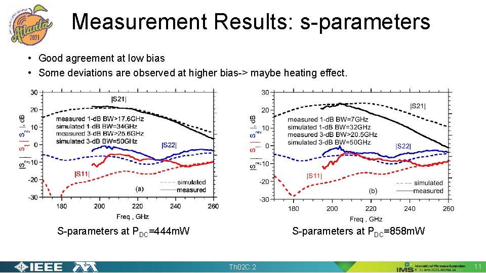
Measurement Results: s-parameters • Good agreement at low bias • Some deviations are observed at higher bias-> maybe heating effect. S-parameters at PDC=444 m. W S-parameters at PDC=858 m. W Th 02 C. 2 11

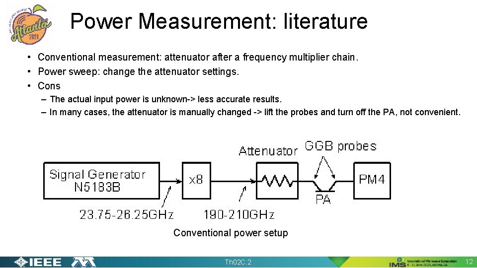
Power Measurement: literature • Conventional measurement: attenuator after a frequency multiplier chain. • Power sweep: change the attenuator settings. • Cons – The actual input power is unknown-> less accurate results. – In many cases, the attenuator is manually changed -> lift the probes and turn off the PA, not convenient. Conventional power setup Th 02 C. 2 12

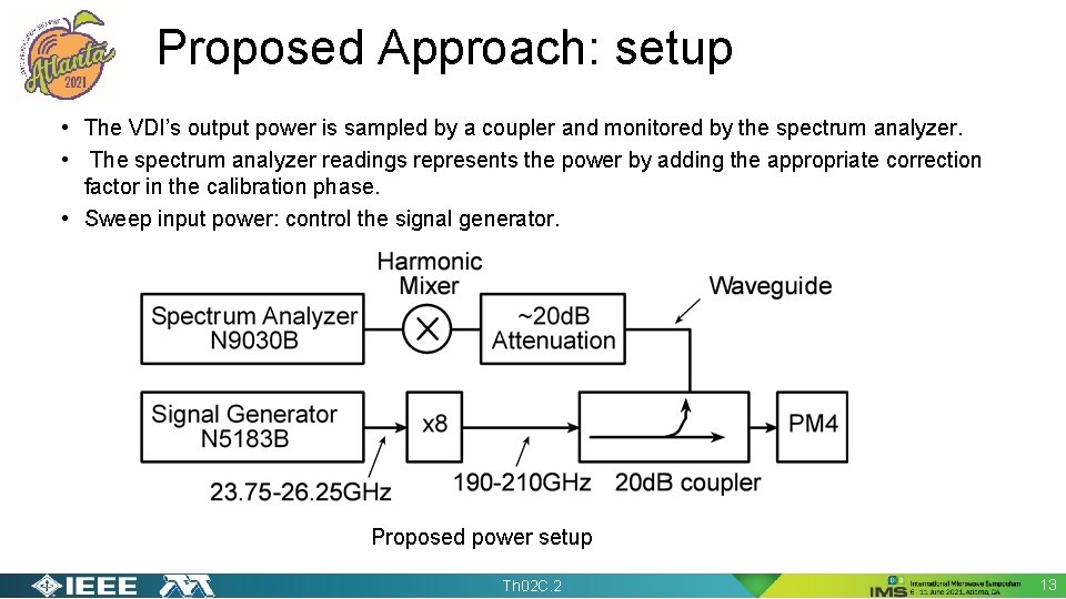
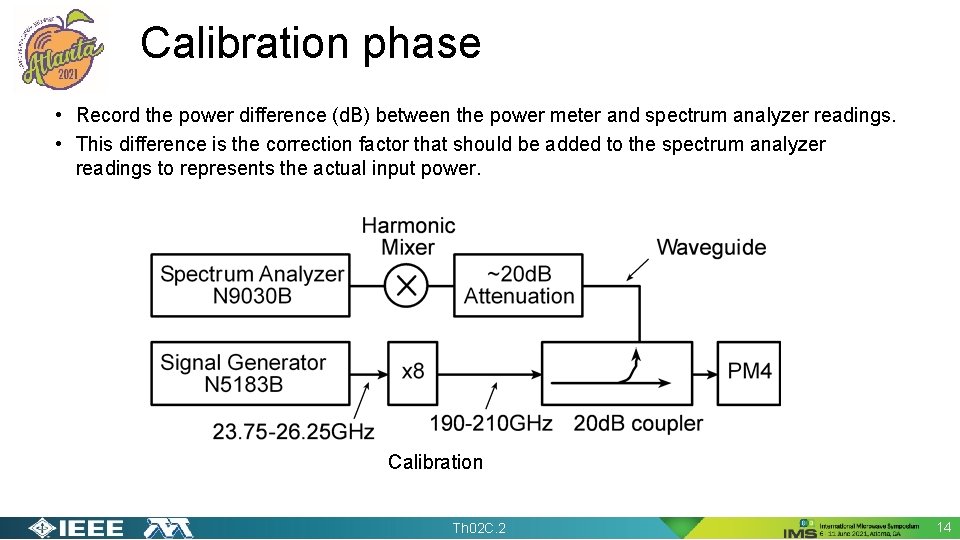
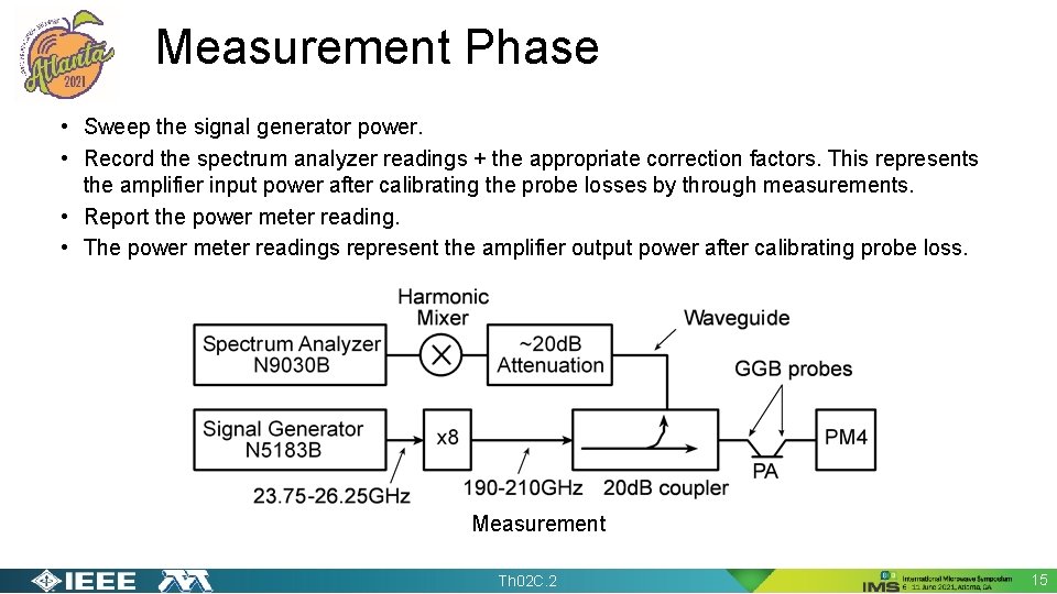
Proposed Approach: setup • The VDI’s output power is sampled by a coupler and monitored by the spectrum analyzer. • The spectrum analyzer readings represents the power by adding the appropriate correction factor in the calibration phase. • Sweep input power: control the signal generator. Proposed power setup Th 02 C. 2 13

Calibration phase • Record the power difference (d. B) between the power meter and spectrum analyzer readings. • This difference is the correction factor that should be added to the spectrum analyzer readings to represents the actual input power. Calibration Th 02 C. 2 14

Measurement Phase • Sweep the signal generator power. • Record the spectrum analyzer readings + the appropriate correction factors. This represents the amplifier input power after calibrating the probe losses by through measurements. • Report the power meter reading. • The power meter readings represent the amplifier output power after calibrating probe loss. Measurement Th 02 C. 2 15

Pros of this measurement approach • Accurate gain measurement even at very low input power. • Power is swept by the signal generator -> Extremely convenient since all the measurements are done without lifting the probes or turn off the PA bias. Th 02 C. 2 16

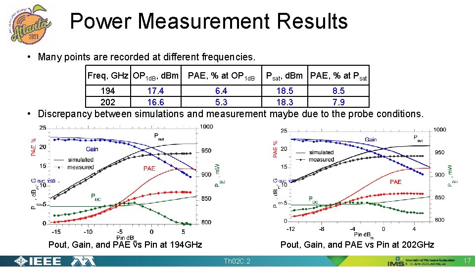
Power Measurement Results • Many points are recorded at different frequencies. Freq, GHz OP 1 d. B, d. Bm 194 202 PAE, % at OP 1 d. B 17. 4 16. 6 6. 4 5. 3 Psat, d. Bm PAE, % at Psat 18. 5 18. 3 8. 5 7. 9 • Discrepancy between simulations and measurement maybe due to the probe conditions. Pout, Gain, and PAE vs Pin at 194 GHz Pout, Gain, and PAE vs Pin at 202 GHz Th 02 C. 2 17

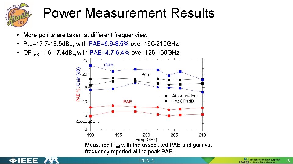
Power Measurement Results • More points are taken at different frequencies. • Psat=17. 7 -18. 5 d. Bm, with PAE=6. 9 -8. 5% over 190 -210 GHz • OP 1 d. B =16 -17. 4 d. Bm with PAE=4. 7 -6. 4% over 125 -150 GHz Measured Pout with the associated PAE and gain vs. frequency reported at the peak PAE. Th 02 C. 2 18

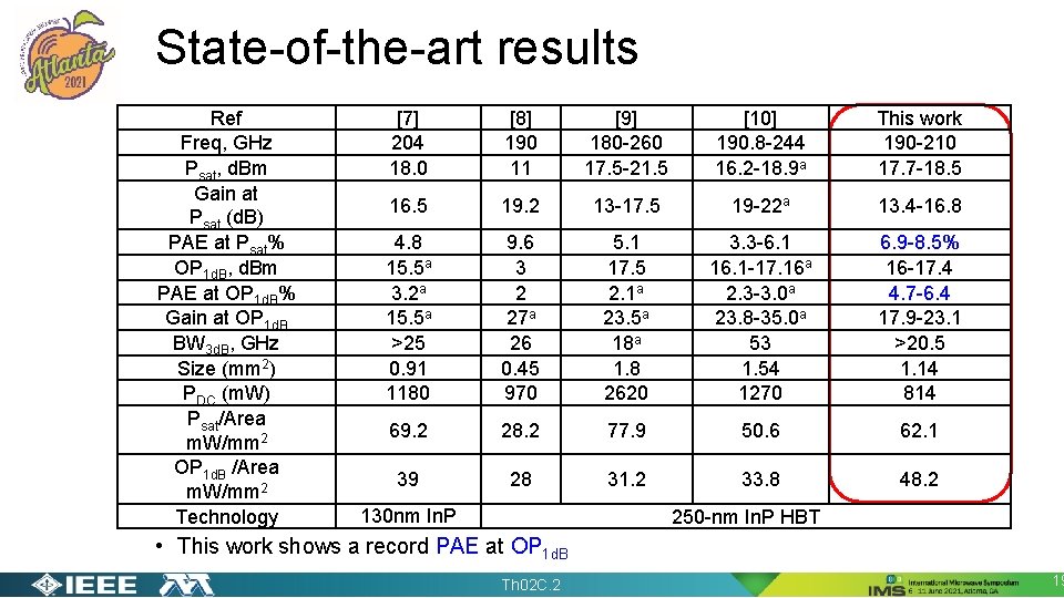
State-of-the-art results Ref Freq, GHz Psat, d. Bm Gain at Psat (d. B) PAE at Psat% OP 1 d. B, d. Bm PAE at OP 1 d. B% Gain at OP 1 d. B BW 3 d. B, GHz Size (mm 2) PDC (m. W) Psat/Area m. W/mm 2 OP 1 d. B /Area m. W/mm 2 Technology [7] 204 18. 0 [8] 190 11 [9] 180 -260 17. 5 -21. 5 [10] 190. 8 -244 16. 2 -18. 9 a This work 190 -210 17. 7 -18. 5 16. 5 19. 2 13 -17. 5 19 -22 a 13. 4 -16. 8 4. 8 15. 5 a 3. 2 a 15. 5 a >25 0. 91 1180 9. 6 3 2 27 a 26 0. 45 970 5. 1 17. 5 2. 1 a 23. 5 a 18 a 1. 8 2620 3. 3 -6. 1 16. 1 -17. 16 a 2. 3 -3. 0 a 23. 8 -35. 0 a 53 1. 54 1270 6. 9 -8. 5% 16 -17. 4 4. 7 -6. 4 17. 9 -23. 1 >20. 5 1. 14 814 69. 2 28. 2 77. 9 50. 6 62. 1 39 28 31. 2 33. 8 48. 2 130 nm In. P 250 -nm In. P HBT • This work shows a record PAE at OP 1 d. B Th 02 C. 2 19

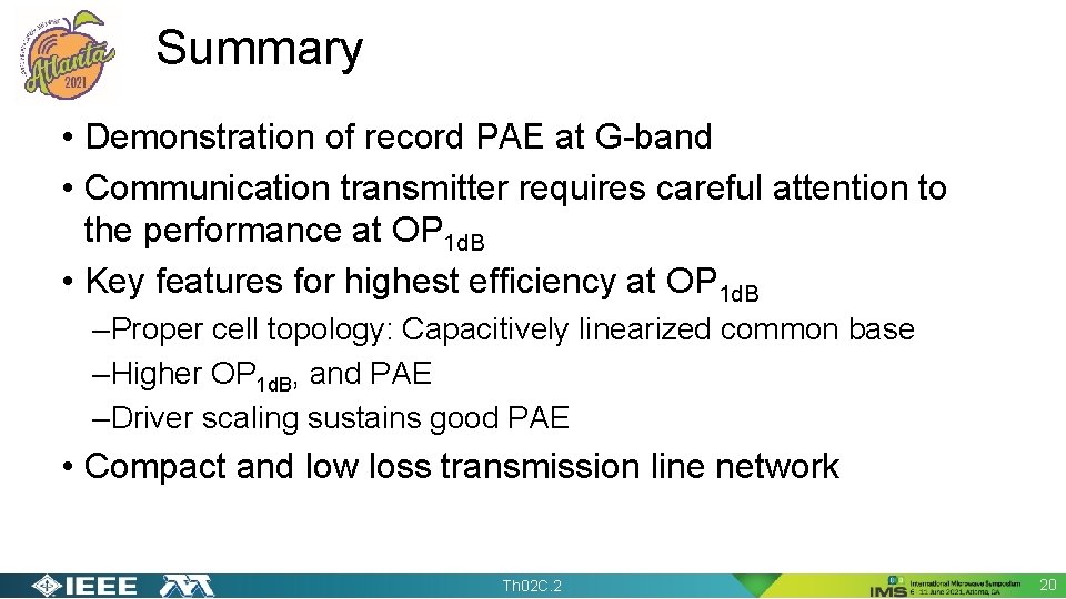
Summary • Demonstration of record PAE at G-band • Communication transmitter requires careful attention to the performance at OP 1 d. B • Key features for highest efficiency at OP 1 d. B – Proper cell topology: Capacitively linearized common base – Higher OP 1 d. B, and PAE – Driver scaling sustains good PAE • Compact and low loss transmission line network Th 02 C. 2 20

Acknowledgement • This work was supported in part by the Semiconductor Research Corporation and DARPA under the JUMP program. • The authors thank Teledyne Scientific & Imaging for the IC fabrication. Th 02 C. 2 21

Thank You Th 02 C. 2 22
![References 1 M J W Rodwell et al 100 340 GHz Systems References [1] M. J. W. Rodwell et al. , “ 100 -340 GHz Systems:](https://slidetodoc.com/presentation_image_h2/9a864fe23005c5b9d1c50b00c56c598e/image-23.jpg)
References [1] M. J. W. Rodwell et al. , “ 100 -340 GHz Systems: Transistors and Applications, ” in Proc. IEEE IEDM, 2018, pp. 14. 3. 1 -14. 3. 4. [2] H. Bameri and O. Momeni, "An Embedded 200 GHz Power Amplifier with 9. 4 d. Bm Saturated Power and 19. 5 d. B Gain in 65 nm CMOS, " in Proc. RFIC 2020, pp. 191 -194 [3] M. H. Eissa and D. Kissinger, "4. 5 A 13. 5 d. Bm Fully Integrated 200 -to-255 GHz Power Amplifier with a 4 -Way Power Combiner in Si. Ge: C Bi. CMOS, " 2019 IEEE International Solid- State Circuits Conference - (ISSCC), San Francisco, CA, USA, 2019, pp. 82 -84. [4] M. Ćwikliński et al. , "D-Band G-Band High-Performance Ga. N Power Amplifier MMICs, " in IEEE Trans. Microw. Theory Techn. , vol. 67, no. 12, pp. 5080 -5089, Dec. 2019. [5] M. Ćwikliński et al. , "First Demonstration of G-Band Broadband Ga. N Power Amplifier MMICs Operating Beyond 200 GHz, " 2020 IEEE/MTT-S International Microwave Symposium (IMS), Los Angeles, CA, USA, 2020, pp. 1117 -1120. [6] M. Urteaga, Z. Griffith, M. Seo, J. Hacker, M. Rodwell, “In. P HBT Technologies for THz Integrated Circuits”, Proc. of the IEEE, vol. 105, no. 6, pp 1051 -1067, June 2017. [7] A. S. H. Ahmed, A. A. Farid, M. Urteaga and M. J. W. Rodwell, "204 GHz Stacked-Power Amplifiers Designed by a Novel Two-Port Technique, " 2018 13 th European Microwave Integrated Circuits Conference (Eu. MIC), Madrid, 2018, pp. 29 -32. [8] Z. Griffith, M. Urteaga and P. Rowell, "A 190 -GHz High-Gain, 3 -d. Bm OP 1 d. B Low DC-Power Amplifier in 250 -nm In. P HBT, " in IEEE MWCL, vol. 27, pp. 1128 -1130, Dec. 2017. [9] Z. Griffith, M. Urteaga and P. Rowell, "180– 265 GHz, 17– 24 d. Bm output power broadband, high-gain power amplifiers in In. P HBT, " 2017 IEEE MTT-S International Microwave Symposium (IMS), Honololu, HI, 2017, pp. 973 -976. [10] Z. Griffith, M. Urteaga, P. Rowell, and R. Pierson, “A 50– 80 m. W SSPA from 190. 8– 244 GHz at 0. 5 m. W pin, ” in Proc. IMS 2014, pp. 1– 4. [11] V. Radisic, D. W. Scott, A. Cavus, and C. Monier, “ 220 -GHz high-efficiency In. P HBT power amplifiers, ” IEEE Trans. Microw. Theory Techn. , vol. 62, no. 12, pp. 3001– 3005, Dec. 2014. [12] T. B. Reed, Z. Griffith, P. Rowell, M. Field, and M. Rodwell, "A 180 m. W In. P HBT power amplifier MMIC at 214 GHz, " in 2013 IEEE Compound Semiconductor Integrated Circuit Symposium, Monterey, CA, Oct. 2013, pp. I-4. [13] M. Bao, V. Vassilev, D. Gustafsson and H. Zirath, "G-band Power Amplifiers in 130 nm In. P Technology, " 2020 15 th European Microwave Integrated Circuits Conference (Eu. MIC), Utrecht, Netherlands, 2021, pp. 5 -8. [14] A. S. H. Ahmed, M. Seo, A. A. Farid, M. Urteaga, J. F. Buckwalter and M. J. W. Rodwell, "A 140 GHz power amplifier with 20. 5 d. Bm output power and 20. 8% PAE in 250 -nm In. P HBT technology, " 2020 IEEE/MTT-S International Microwave Symposium (IMS), Los Angeles, CA, USA, 2020, pp. 492 -495. [15] A. S. H. Ahmed, M. Seo, A. A. Farid, M. Urteaga, J. F. Buckwalter and M. J. W. Rodwell, "A 200 m. W D-band Power Amplifier with 17. 8% PAE in 250 -nm In. P HBT Technology, " 2020 15 th European Microwave Integrated Circuits Conference (Eu. MIC), Utrecht, Netherlands, 2021, pp. 1 -4. [16] M. Seo, A. S. H. Ahmed, U. Soylu, A. A. Farid, Y. Na, and M. J. W. Rodwell, "A 200 GHz In. P HBT Direct-Conversion LO-Phase-Shifted Transmitter/Receiver with 15 d. Bm Output Power, " submitted to 2021 IEEE Radio Frequency Integrated Circuits Symposium (RFIC), Atlanta, GA. [17] A. S. H. Ahmed, U. Soylu, M. Seo, Miguel Urteaga and M. J. W. Rodwell, " A compact H-band Power Amplifier with High Output Power, " submitted to 2021 IEEE/MTT-S International Microwave Symposium (IMS), Atlanta, GA. [18] A. S. H. Ahmed, A. Simsek, M. Urteaga and M. J. W. Rodwell, "8. 6 -13. 6 m. W Series-Connected Power Amplifiers Designed at 325 GHz Using 130 nm In. P HBT Technology, " 2018 IEEE Bi. CMOS and Compound Semiconductor Integrated Circuits and Technology Symposium (BCICTS), San Diego, CA, USA, 2018, pp. 164 -167. Th 02 C. 2 23

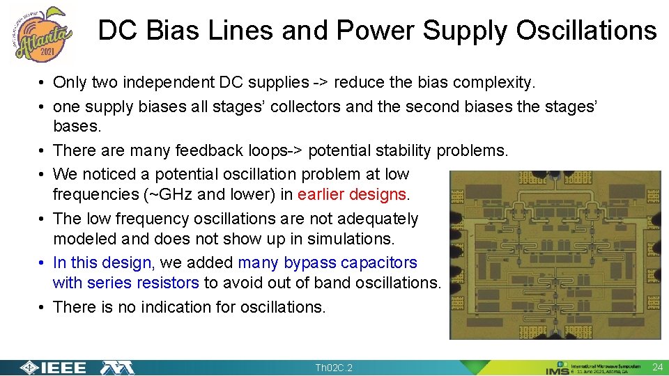
DC Bias Lines and Power Supply Oscillations • Only two independent DC supplies -> reduce the bias complexity. • one supply biases all stages’ collectors and the second biases the stages’ bases. • There are many feedback loops-> potential stability problems. • We noticed a potential oscillation problem at low frequencies (~GHz and lower) in earlier designs. • The low frequency oscillations are not adequately modeled and does not show up in simulations. • In this design, we added many bypass capacitors with series resistors to avoid out of band oscillations. • There is no indication for oscillations. Th 02 C. 2 24

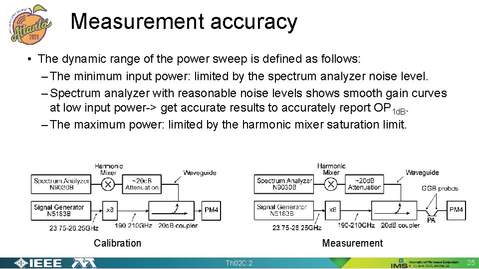
Measurement accuracy • The dynamic range of the power sweep is defined as follows: – The minimum input power: limited by the spectrum analyzer noise level. – Spectrum analyzer with reasonable noise levels shows smooth gain curves at low input power-> get accurate results to accurately report OP 1 d. B. – The maximum power: limited by the harmonic mixer saturation limit. Calibration Measurement Th 02 C. 2 25

Measurement accuracy • Probe losses are calibrated by through measurement. • Old probes show non-50 W impedance which degrades the output power. • So, the probes may contribute to higher losses than the one measured in the through measurement. • We did the measurement with an old probe pair, and we believe that the results could be improved by a newer one. Th 02 C. 2 26