Update of CLIC accelerating structure design Hao Zha
- Slides: 19

Update of CLIC accelerating structure design Hao Zha, Alexej Grudiev 18/01/2015

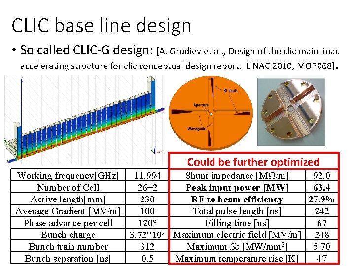
CLIC base line design • So called CLIC-G design: [A. Grudiev et al. , Design of the clic main linac accelerating structure for clic conceptual design report, LINAC 2010, MOP 068]. Could be further optimized Working frequency[GHz] 11. 994 Shunt impedance [MΩ/m] 92. 0 Number of Cell 26+2 Peak input power [MW] 63. 4 Active length[mm] 230 RF to beam efficiency 27. 9% Average Gradient [MV/m] 100 Total pulse length [ns] 242 Phase advance per cell 120° Filling time [ns] 67 Bunch charge 3. 72*109 Maximum electric field [MV/m] 248 Bunch train number 312 Maximum Sc [MW/mm 2] 5. 70 Bunch separation [ns] 0. 5 Maximum temperature rise [K] 47

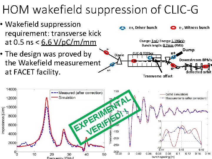
HOM wakefield suppression of CLIC-G • Wakefield suppression requirement: transverse kick at 0. 5 ns < 6. 6 V/p. C/m/mm • The design was proved by the Wakefield measurement at FACET facility. e-, Witness bunch e+, Driver bunch Charge: 3 n. C; Energy: 1. 19 Ge. V; Bunch length: 0. 7 mm (RMS) e- Dipole CLIC-G TD 26 cc e+ Dump Downstream BPMs e+ L A T N E !! M I D R E E IFI P EX VER e. Transverse offset deflected orbit

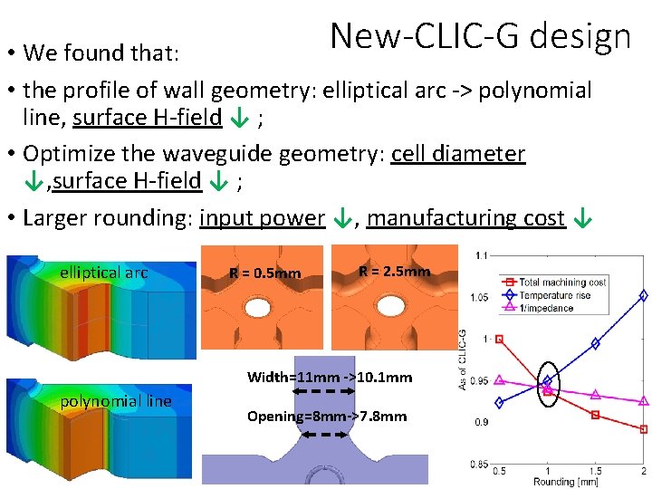
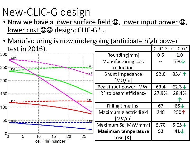
New-CLIC-G design • We found that: • the profile of wall geometry: elliptical arc -> polynomial line, surface H-field ↓ ; • Optimize the waveguide geometry: cell diameter ↓, surface H-field ↓ ; • Larger rounding: input power ↓, manufacturing cost ↓ elliptical arc R = 0. 5 mm R = 2. 5 mm Width=11 mm ->10. 1 mm polynomial line Opening=8 mm->7. 8 mm

New-CLIC-G design • Now we have a lower surface field , lower input power , lower cost design: CLIC-G*. • Manufacturing is now undergoing (anticipate high power CLIC-G* test in 2016). Rounding[mm] 0. 5 Manufacturing cost -reduction Shunt impedance 92. 0 [MΩ/m] Peak input power [MW] 63. 4 RF to beam efficiency 27. 9% Filling time [ns] Maximum electric field [MV/m] Maximum Sc [MW/mm 2] Maximum temperature rise [K] 1. 0 7%↓ 95. 4↑ 67 248 62. 3↓ 28. 4% ↑ 66↓ 250↑ 5. 70 52 5. 65↓ 41↓

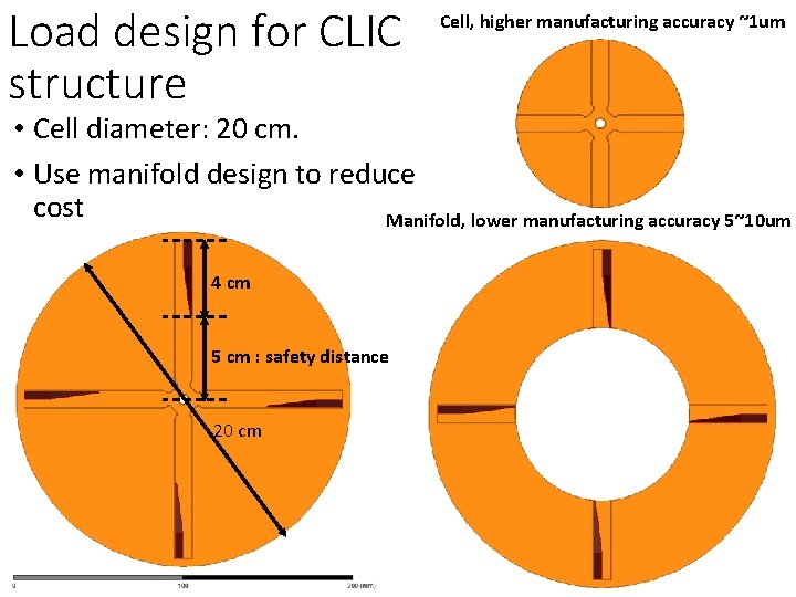
Load design for CLIC structure Cell, higher manufacturing accuracy ~1 um • Cell diameter: 20 cm. • Use manifold design to reduce cost Manifold, lower manufacturing accuracy 5~10 um 4 cm 5 cm : safety distance 20 cm

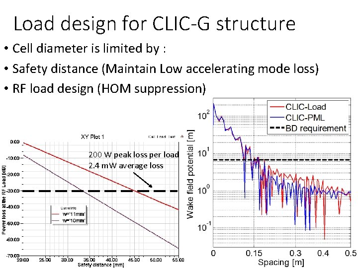
Load design for CLIC-G structure • Cell diameter is limited by : • Safety distance (Maintain Low accelerating mode loss) • RF load design (HOM suppression) 200 W peak loss per load 2. 4 m. W average loss

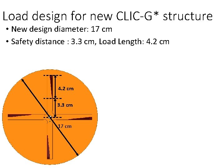
Load design for new CLIC-G* structure • New design diameter: 17 cm • Safety distance : 3. 3 cm, Load Length: 4. 2 cm 3. 3 cm 17 cm

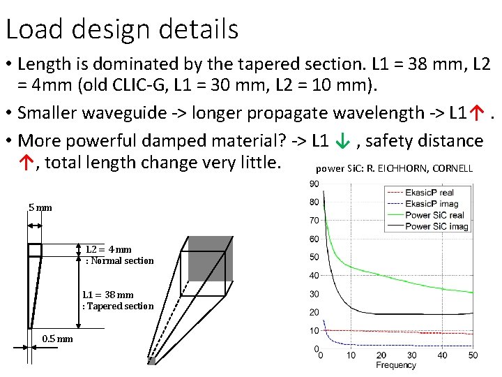
Load design details • Length is dominated by the tapered section. L 1 = 38 mm, L 2 = 4 mm (old CLIC-G, L 1 = 30 mm, L 2 = 10 mm). • Smaller waveguide -> longer propagate wavelength -> L 1↑. • More powerful damped material? -> L 1 ↓ , safety distance ↑, total length change very little. power Si. C: R. EICHHORN, CORNELL 5 mm L 2 = 4 mm : Normal section L 1 = 38 mm : Tapered section 0. 5 mm

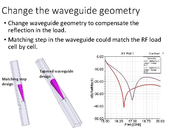
Change the waveguide geometry • Change waveguide geometry to compensate the reflection in the load. • Matching step in the waveguide could match the RF load cell by cell. Matching step design Tapered waveguide design

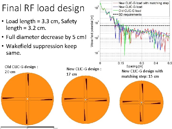
Final RF load design • Load length = 3. 3 cm, Safety length = 3. 2 cm. • Full diameter decrease by 5 cm! • Wakefield suppression keep same. Old CLIC-G design : 20 cm New CLIC-G design : 17 cm New CLIC-G design with matching step: 15 cm

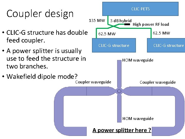
CLIC PETS Coupler design 135 MW • CLIC-G structure has double feed coupler. • A power splitter is usually use to feed the structure in two branches. • Wakefield dipole mode? 3 d. B hybrid High power RF load 62. 5 MW CLIC-G structure HOM waveguide Coupler waveguide HOM waveguide A power splitter here ?

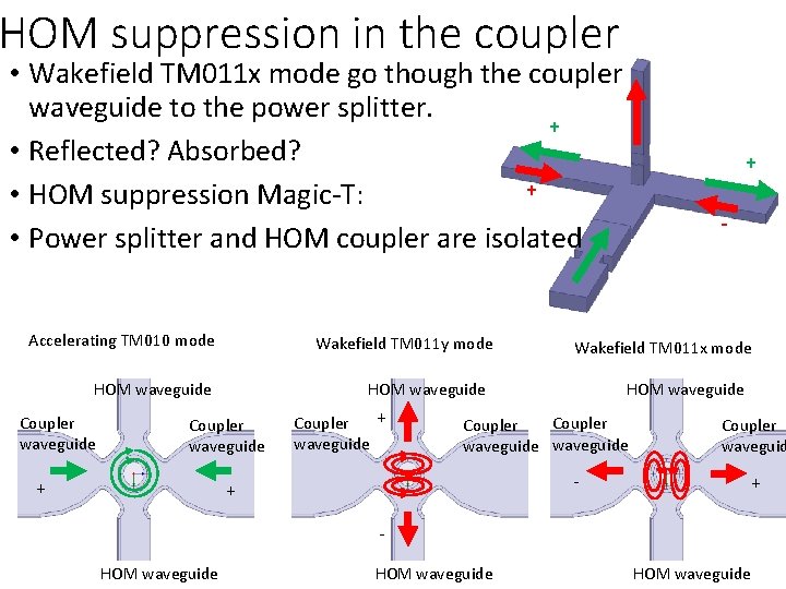
HOM suppression in the coupler • Wakefield TM 011 x mode go though the coupler waveguide to the power splitter. + • Reflected? Absorbed? + • HOM suppression Magic-T: • Power splitter and HOM coupler are isolated Accelerating TM 010 mode Wakefield TM 011 y mode HOM waveguide Coupler waveguide + + Coupler waveguide - Wakefield TM 011 x mode HOM waveguide Coupler waveguide + HOM waveguide Coupler waveguide - + Coupler waveguid + HOM waveguide

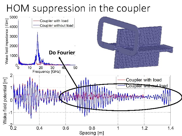
HOM suppression in the coupler Do Fourier

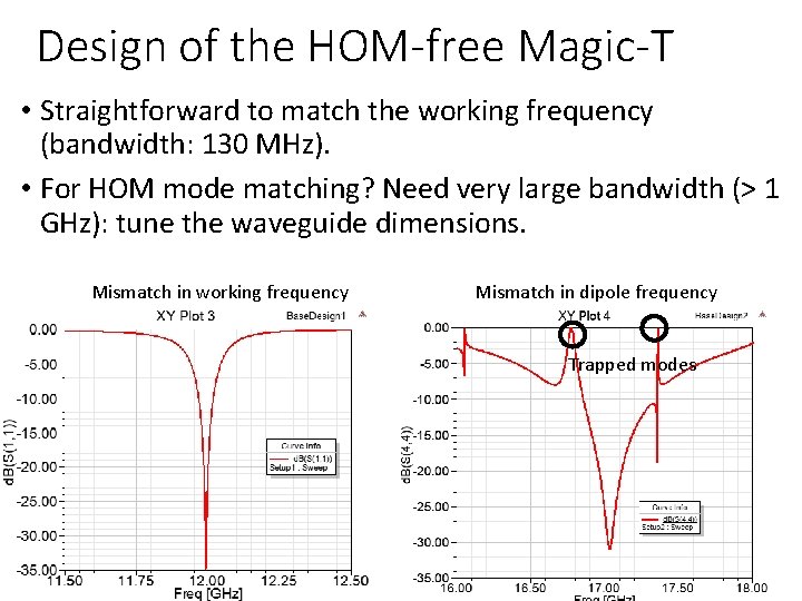
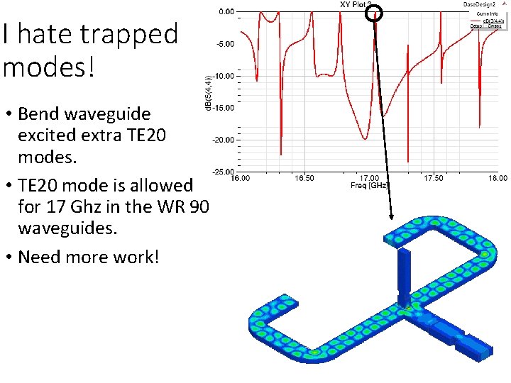
Design of the HOM-free Magic-T • Straightforward to match the working frequency (bandwidth: 130 MHz). • For HOM mode matching? Need very large bandwidth (> 1 GHz): tune the waveguide dimensions. Mismatch in working frequency Mismatch in dipole frequency Trapped modes

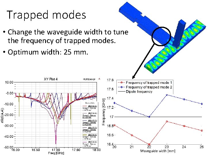
Trapped modes • Change the waveguide width to tune the frequency of trapped modes. • Optimum width: 25 mm.

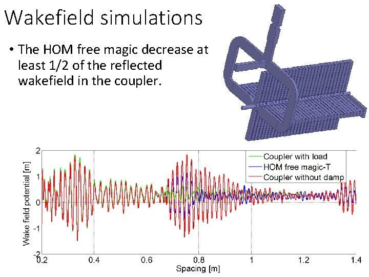
Wakefield simulations • The HOM free magic decrease at least 1/2 of the reflected wakefield in the coupler.

I hate trapped modes! • Bend waveguide excited extra TE 20 modes. • TE 20 mode is allowed for 17 Ghz in the WR 90 waveguides. • Need more work!

Summary • We’ve almost finished the new CLIC accelerating structure design: • Better RF parameters of the structure • Lower machining cost • Compact transverse dimensions and RF loads. • HOM-free magic-T for the power coupling.