Unit 3 Logic Function Realization with MSI Circuits
- Slides: 17

Unit – 3 Logic Function Realization with MSI Circuits Hardik Doshi � 99789 11553 �hardik. doshi@darshan. ac. in Digital Electronics (2131004) Darshan Institute of Engineering & Technology

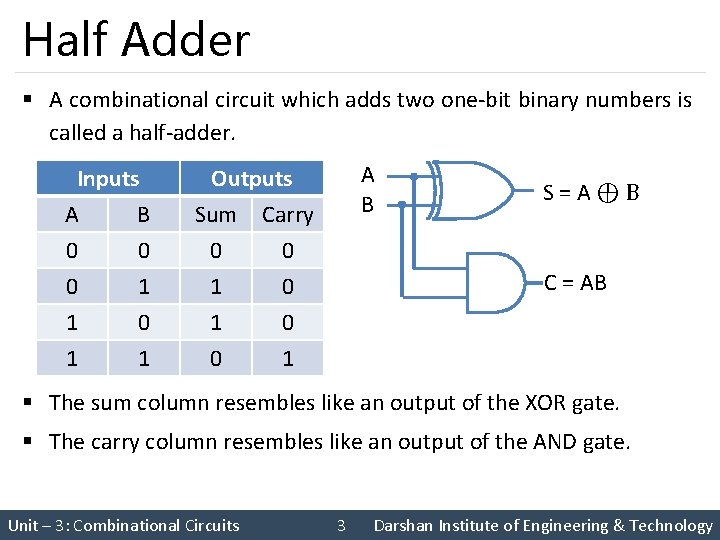
Half Adder § A combinational circuit which adds two one-bit binary numbers is called a half-adder. Inputs A B 0 0 0 1 1 1 0 1 A B Outputs Sum Carry 0 0 1 0 S=A⊕B C = AB 0 1 § The sum column resembles like an output of the XOR gate. § The carry column resembles like an output of the AND gate. Unit – 3: Combinational Circuits 3 Darshan Institute of Engineering & Technology

Limitation of Half-Adder § In multi-digit addition we have to add two bits along with the carry of previous digit addition. Such addition requires addition of 3 bits. This is not possible in half-adders. Unit – 3: Combinational Circuits 4 Darshan Institute of Engineering & Technology

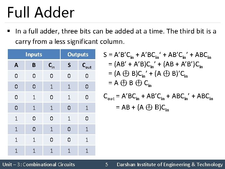
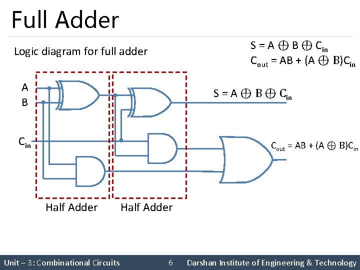
Full Adder § In a full adder, three bits can be added at a time. The third bit is a carry from a less significant column. Inputs Outputs A B Cin S Cout 0 0 0 0 1 1 0 0 1 0 1 1 1 0 0 1 1 1 Unit – 3: Combinational Circuits S = A’B’Cin + A’BCin‘ + AB’Cin’ + ABCin = (AB’ + A’B)Cin’ + (AB + A’B’)Cin = (A ⊕ B)Cin’ + (A ⊕ B)’Cin = A ⊕ B ⊕ Cin Cout = A’BCin + AB’Cin + ABCin’ + ABCin = AB + (A ⊕ B)Cin 5 Darshan Institute of Engineering & Technology

Full Adder S = A ⊕ B ⊕ Cin Cout = AB + (A ⊕ B)Cin Logic diagram for full adder A B S = A ⊕ B ⊕ Cin Cout = AB + (A ⊕ B)Cin Half Adder Unit – 3: Combinational Circuits Half Adder 6 Darshan Institute of Engineering & Technology

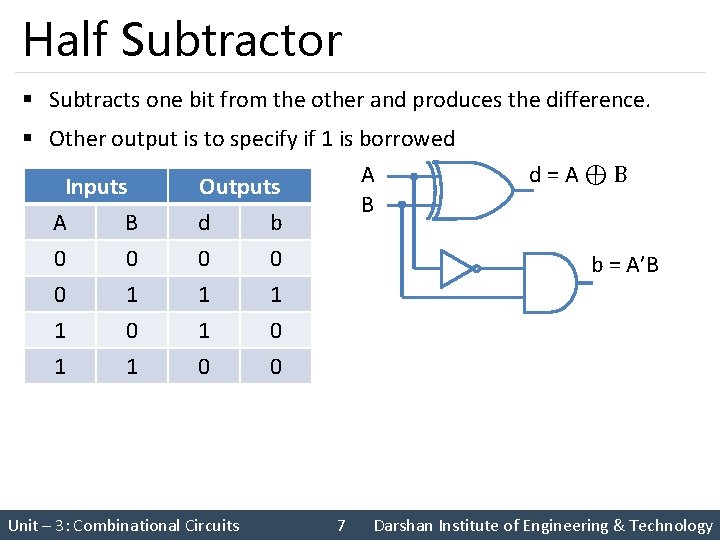
Half Subtractor § Subtracts one bit from the other and produces the difference. § Other output is to specify if 1 is borrowed A Inputs Outputs B A B d b 0 0 0 1 1 0 0 Unit – 3: Combinational Circuits 7 d=A⊕B b = A’B Darshan Institute of Engineering & Technology

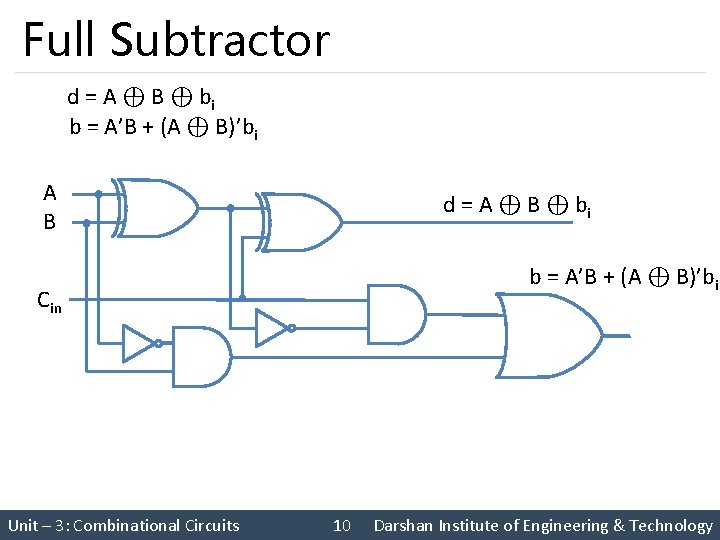
Full Subtractor § Half subtractor can be used only for LSB subtraction. § Borrow from LSBs affects the subtraction in the next higher column. § Subtrahend bit is subtracted from minuend and consider borrow if generated from preceding column. § Full subtractor is a combinational circuit with 3 inputs (A, B, bi) § Subtraction = A – B – bi Unit – 3: Combinational Circuits 8 Darshan Institute of Engineering & Technology

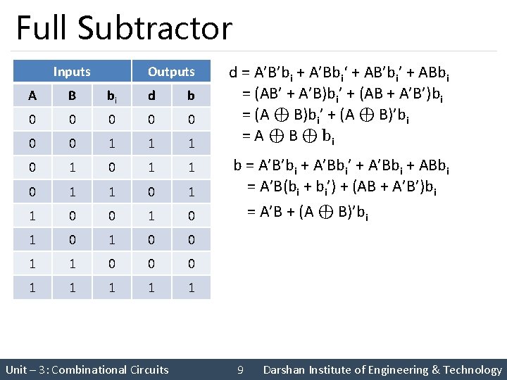
Full Subtractor Inputs Outputs A B bi d b 0 0 0 0 1 1 1 0 1 1 0 0 1 0 1 0 0 1 1 0 0 0 1 1 1 Unit – 3: Combinational Circuits d = A’B’bi + A’Bbi‘ + AB’bi’ + ABbi = (AB’ + A’B)bi’ + (AB + A’B’)bi = (A ⊕ B)bi’ + (A ⊕ B)’bi = A ⊕ B ⊕ bi b = A’B’bi + A’Bbi’ + A’Bbi + ABbi = A’B(bi + bi’) + (AB + A’B’)bi = A’B + (A ⊕ B)’bi 9 Darshan Institute of Engineering & Technology

Full Subtractor d = A ⊕ B ⊕ bi b = A’B + (A ⊕ B)’bi A B d = A ⊕ B ⊕ bi b = A’B + (A ⊕ B)’bi Cin Unit – 3: Combinational Circuits 10 Darshan Institute of Engineering & Technology

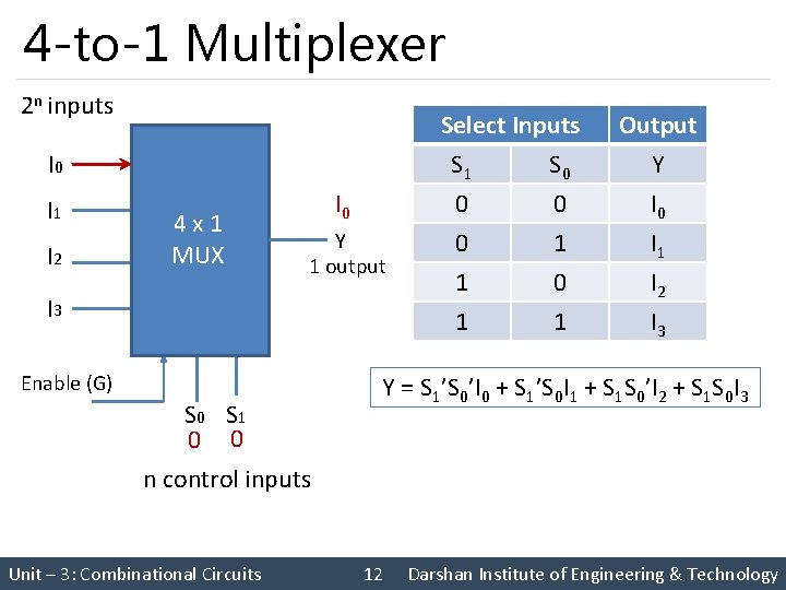
Multiplexer § A multiplexer(MUX) is a device that allows digital information from several sources to be routed onto a single line for transmission over that line to a common destination. § Consider an integer ‘m’, which is constrained by the following relation: m = 2 n, where m and n are both integers. § A m-to-1 Multiplexer has • • m Inputs: I 0, I 1, I 2, . . . . I(m-1) One Output: Y n Control inputs: S 0, S 1, S 2, . . . S(n-1) One (or more) Enable input(s) such that Y may be equal to one of the inputs, depending upon the control inputs. Unit – 3: Combinational Circuits 11 Darshan Institute of Engineering & Technology

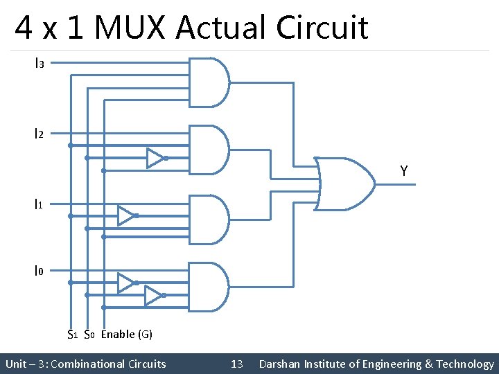
4 -to-1 Multiplexer 2 n inputs I 0 I 1 I 2 4 x 1 MUX I 0 Y 1 output I 3 Enable (G) S 0 S 1 0 0 Select Inputs S 1 S 0 0 1 1 1 0 1 Output Y I 0 I 1 I 2 I 3 Y = S 1’S 0’I 0 + S 1’S 0 I 1 + S 1 S 0’I 2 + S 1 S 0 I 3 n control inputs Unit – 3: Combinational Circuits 12 Darshan Institute of Engineering & Technology

4 x 1 MUX Actual Circuit I 3 I 2 Y I 1 I 0 S 1 S 0 Enable (G) Unit – 3: Combinational Circuits 13 Darshan Institute of Engineering & Technology

Application of Multiplexer § Logic function generation § Data selection § Data routing § Operation sequencing § Parallel-to-serial conversion § Waveform generation Unit – 3: Combinational Circuits 14 Darshan Institute of Engineering & Technology

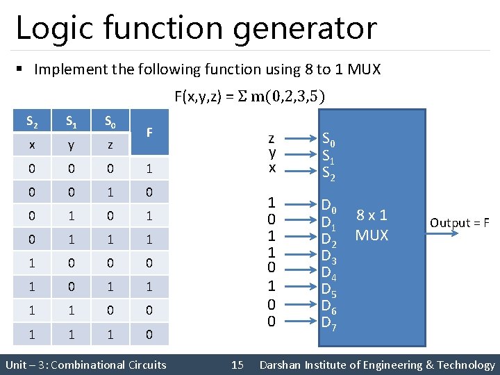
Logic function generator § Implement the following function using 8 to 1 MUX F(x, y, z) = Σ m(0, 2, 3, 5) S 2 S 1 S 0 x y z 0 0 0 1 0 1 1 0 0 0 1 1 1 1 0 0 1 1 1 0 F Unit – 3: Combinational Circuits 15 z y x S 0 S 1 S 2 1 0 1 0 0 D 1 D 2 D 3 D 4 D 5 D 6 D 7 8 x 1 MUX Output = F Darshan Institute of Engineering & Technology

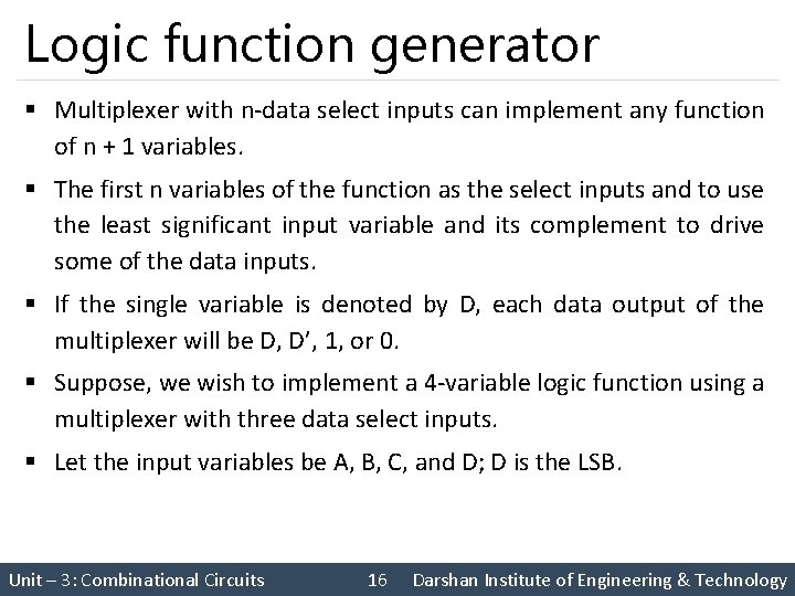
Logic function generator § Multiplexer with n-data select inputs can implement any function of n + 1 variables. § The first n variables of the function as the select inputs and to use the least significant input variable and its complement to drive some of the data inputs. § If the single variable is denoted by D, each data output of the multiplexer will be D, D’, 1, or 0. § Suppose, we wish to implement a 4 -variable logic function using a multiplexer with three data select inputs. § Let the input variables be A, B, C, and D; D is the LSB. Unit – 3: Combinational Circuits 16 Darshan Institute of Engineering & Technology

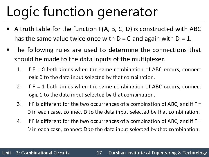
Logic function generator § A truth table for the function F(A, B, C, D) is constructed with ABC has the same value twice once with D = 0 and again with D = 1. § The following rules are used to determine the connections that should be made to the data inputs of the multiplexer. 1. If F = 0 both times when the same combination of ABC occurs, connect logic 0 to the data input selected by that combination. 2. If F = 1 both times when the same combination of ABC occurs, connect logic 1 to the data input selected by that combination. 3. If F is different for the two occurrences of a combination of ABC, and if F = D in each case, connect D to the data input selected by that combination. 4. If F is different for the two occurrences of a combination of ABC, and if F = D in each case, connect D to the data input selected by that combination. Unit – 3: Combinational Circuits 17 Darshan Institute of Engineering & Technology

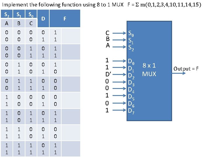
Implement the following function using 8 to 1 MUX F = Σ m(0, 1, 2, 3, 4, 10, 11, 14, 15) S 2 S 1 S 0 A B C 0 0 0 0 1 1 1 F=1 0 0 1 1 0 F = D’ 0 0 1 1 0 1 0 0 F=0 1 1 0 0 0 1 0 0 F=0 1 1 1 F=1 1 1 0 0 0 1 0 0 F=0 1 1 1 F=1 D F C B A S 0 S 1 S 2 1 1 D’ 0 0 1 D 0 D 1 D 2 D 3 D 4 D 5 D 6 D 7 8 x 1 MUX Output = F