Strained Si C C Lee D 91943026 WHY
- Slides: 25
Strained Si C. C. Lee D 91943026
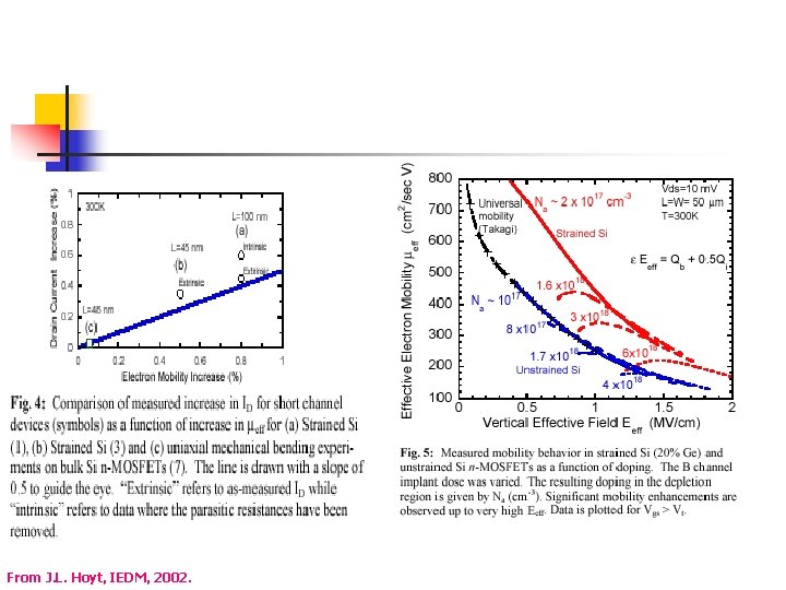
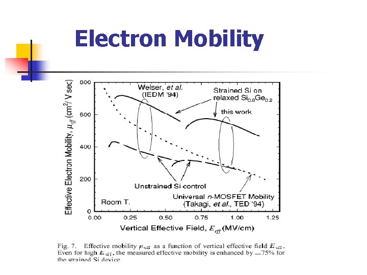
WHY? ØImprovement! Ø Short channel effect (SCE) Ø Gate dielectric thickness Ø Performance state- MOSFET mobility of the strained-Si devices is enhanced by 75% compared to that of the unstrained-Si control devices and the of-the-art universal MOSFET mobility.
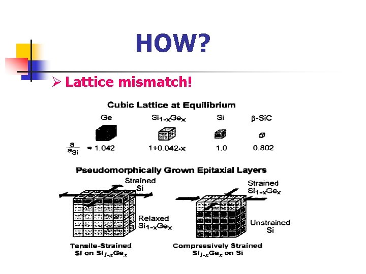
HOW? Ø Lattice mismatch!
Tensile Strain ØEnergy Splitting Diagram
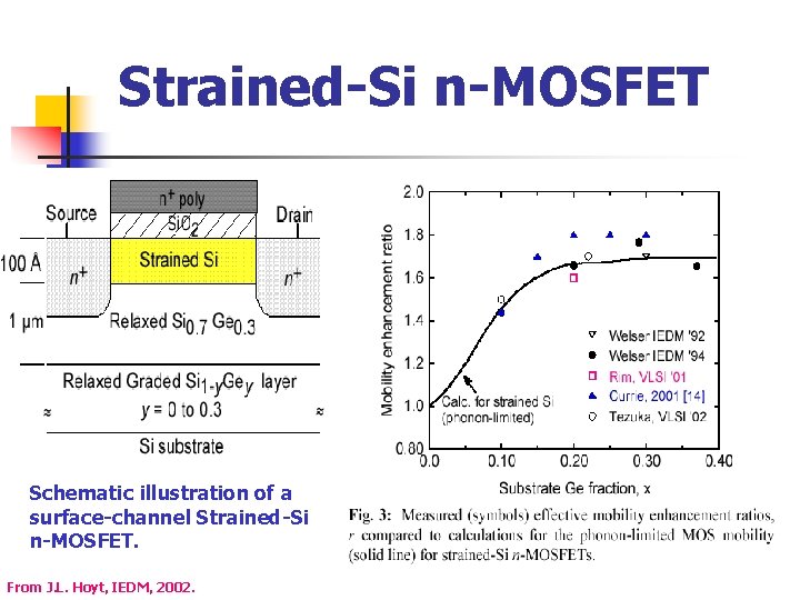
Strained-Si n-MOSFET Schematic illustration of a surface-channel Strained-Si n-MOSFET. From J. L. Hoyt, IEDM, 2002.
From J. L. Hoyt, IEDM, 2002.
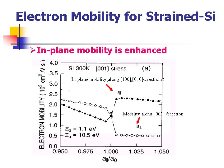
Electron Mobility for Strained-Si ØIn-plane mobility is enhanced In-plane mobility(along [100], [010]directions) Mobility along [001] direction
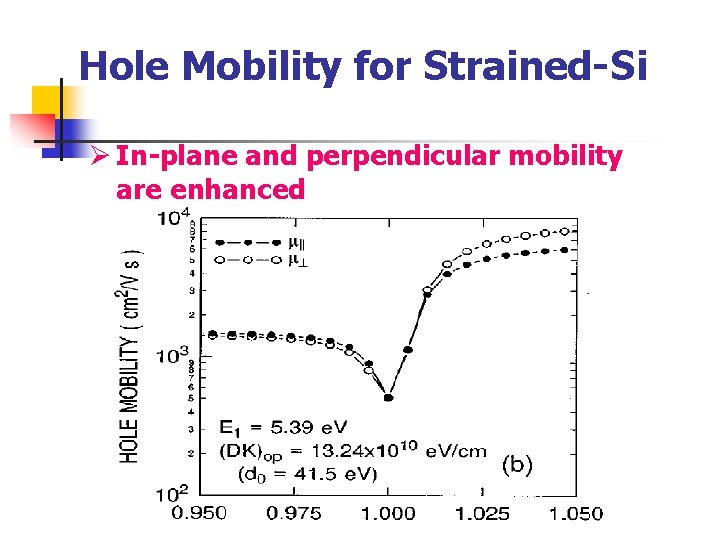
Hole Mobility for Strained-Si Ø In-plane and perpendicular mobility are enhanced
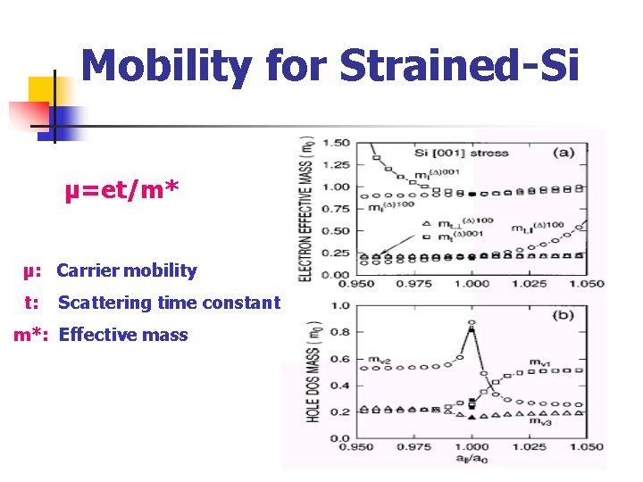
Mobility for Strained-Si µ=et/m* µ: Carrier mobility t: Scattering time constant m*: Effective mass
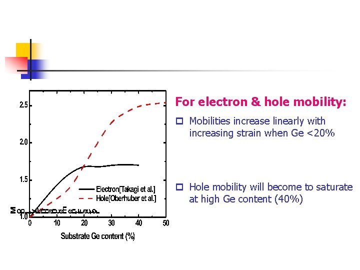
For electron & hole mobility: p Mobilities increase linearly with increasing strain when Ge <20% p Hole mobility will become to saturate at high Ge content (40%)
Electron Mobility
The SOI MOSFETs Ø The advantage of SOI MOSFETs 1. High carrier mobility in channel due to the reduced Coulomb scattering and effective normal field. 2. The reduction of parasitic capacitance of source/drain junctions. 3. Simple isolation process. 4. Small fluctuation of Vt due to low channel impurity concentration.
Si. Ge-On-Insulator Ø The advantage of strained-SOI MOSFETs 1. 2. 3. The SCE can be suppressed by thinning the thickness of Si. Simple isolation process. The reduction of parasitic capacitance of source/drain junctions. => High speed and low power consumption
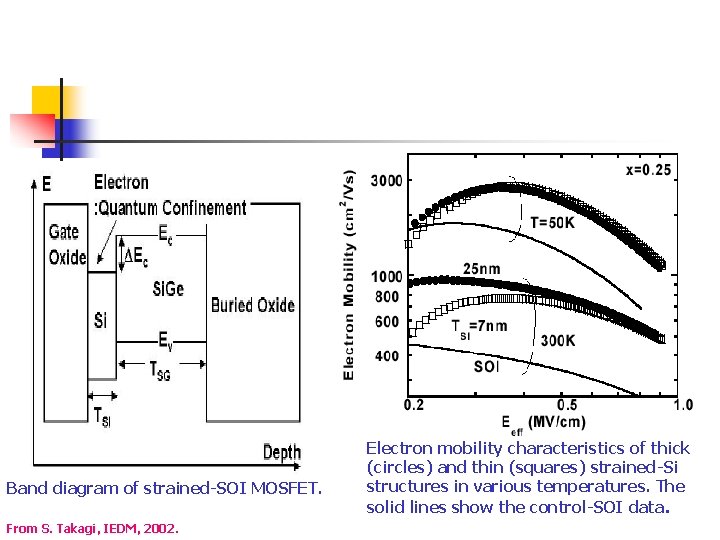
Band diagram of strained-SOI MOSFET. From S. Takagi, IEDM, 2002. Electron mobility characteristics of thick (circles) and thin (squares) strained-Si structures in various temperatures. The solid lines show the control-SOI data.
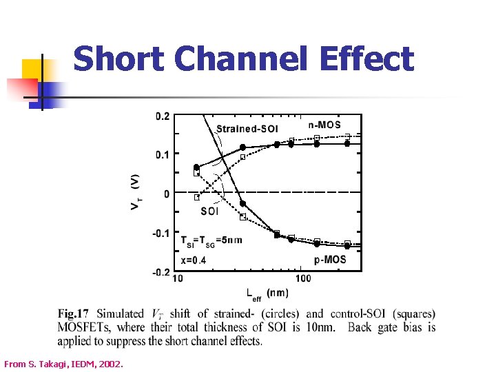
Short Channel Effect From S. Takagi, IEDM, 2002.
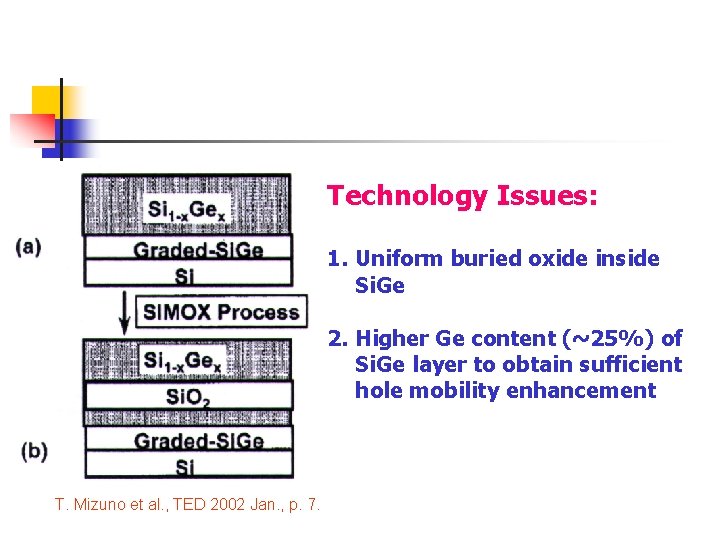
Technology Issues: 1. Uniform buried oxide inside Si. Ge 2. Higher Ge content (~25%) of Si. Ge layer to obtain sufficient hole mobility enhancement T. Mizuno et al. , TED 2002 Jan. , p. 7.
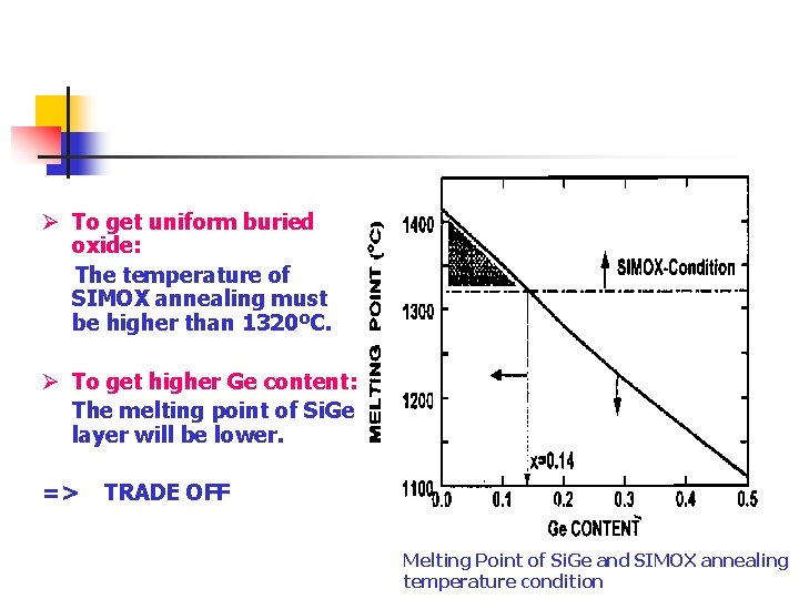
Ø To get uniform buried oxide: The temperature of SIMOX annealing must be higher than 1320ºC. Ø To get higher Ge content: The melting point of Si. Ge layer will be lower. => TRADE OFF Melting Point of Si. Ge and SIMOX annealing temperature condition
Ø How to overcome the trade off? Ø New device structure: Strained-Si on double layer Si. Ge film with different Ge content. Ø New device process: The combination of SIMOX and ITOX
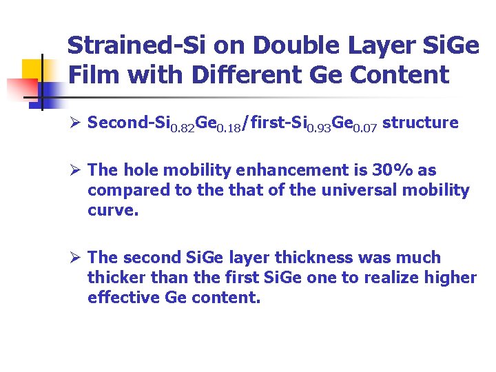
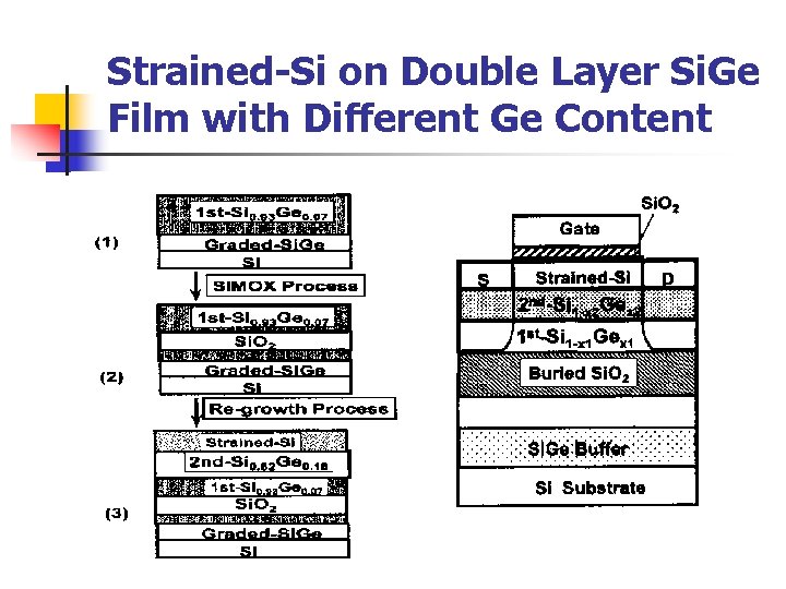
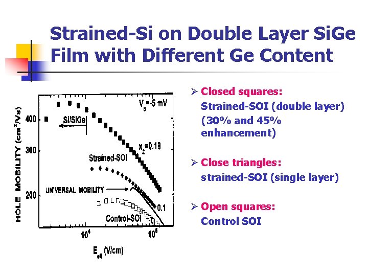
Strained-Si on Double Layer Si. Ge Film with Different Ge Content Ø Second-Si 0. 82 Ge 0. 18/first-Si 0. 93 Ge 0. 07 structure Ø The hole mobility enhancement is 30% as compared to the that of the universal mobility curve. Ø The second Si. Ge layer thickness was much thicker than the first Si. Ge one to realize higher effective Ge content.
Strained-Si on Double Layer Si. Ge Film with Different Ge Content
Strained-Si on Double Layer Si. Ge Film with Different Ge Content Ø Closed squares: Strained-SOI (double layer) (30% and 45% enhancement) Ø Close triangles: strained-SOI (single layer) Ø Open squares: Control SOI
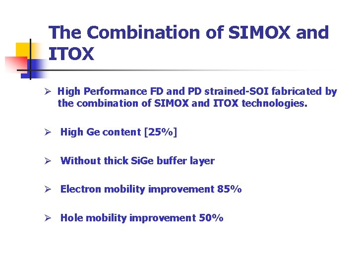
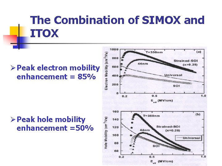
The Combination of SIMOX and ITOX Ø High Performance FD and PD strained-SOI fabricated by the combination of SIMOX and ITOX technologies. Ø High Ge content [25%] Ø Without thick Si. Ge buffer layer Ø Electron mobility improvement 85% Ø Hole mobility improvement 50%
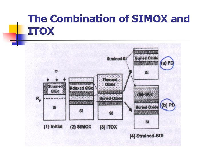
The Combination of SIMOX and ITOX
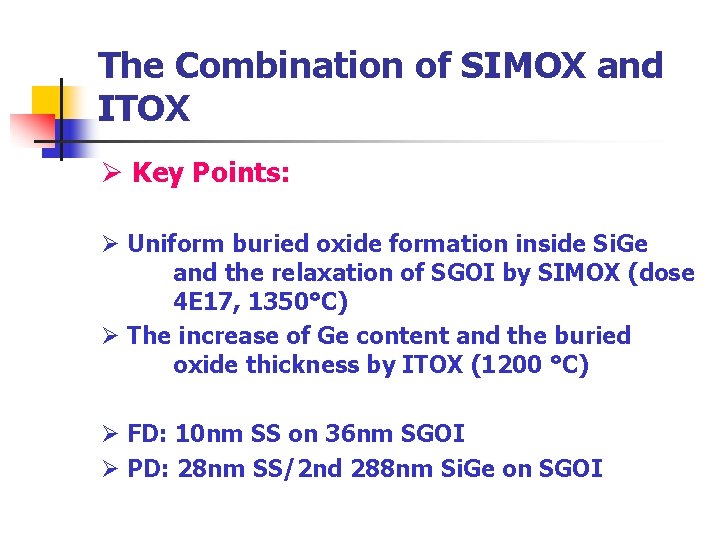
The Combination of SIMOX and ITOX Ø Key Points: Ø Uniform buried oxide formation inside Si. Ge and the relaxation of SGOI by SIMOX (dose 4 E 17, 1350°C) Ø The increase of Ge content and the buried oxide thickness by ITOX (1200 °C) Ø FD: 10 nm SS on 36 nm SGOI Ø PD: 28 nm SS/2 nd 288 nm Si. Ge on SGOI
The Combination of SIMOX and ITOX Ø Peak electron mobility enhancement = 85% Ø Peak hole mobility enhancement =50%