SINGLE PHOTON AVALANCHE DIODE SPAD FROM SINGLE ELEMENT

- Slides: 9

SINGLE PHOTON AVALANCHE DIODE (SPAD): FROM SINGLE ELEMENT TO ARRAY (SPADA) (SWORD) INVASION OF DETECTORS SPADA: an Array of SPAD Detectors for Astrophysical Applications G. Bonanno, M. Belluso, F. Zappa, S. Tisa, S. Cova, P. Maccagnani, D. Bonaccini Calia, R. Saletti, R. Roncella, S. Billota Electro-Optical Characteristics of a SPAD Characterization of SPAD Arrays M. Belluso, G. Bonanno, S. Billotta, A. Calì, S. Scuderi, M. Mazzillo, P. G. Fallica, D. Sanfilippo, E. Sciacca, S. Lombardo INAF – Catania Astrophysical Observatory Dept. of Electronics, Politecnico di Milano ESO European Southern Observatory MANUFACTURERS: ST Microelectronics R&D of Catania IMM-CNR R&D of Catania Dept. of Information Engineering, Pisa Taormina, 2005 Scientific Detectors Workshop LAMEL, IMM-CNR R&D of Bologna University

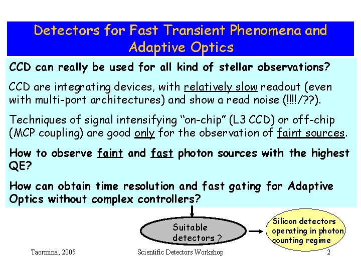
Detectors for Fast Transient Phenomena and Adaptive Optics CCD can really be used for all kind of stellar observations? CCD are integrating devices, with relatively slow readout (even with multi-port architectures) and show a read noise (!!!!/? ? ). Techniques of signal intensifying “on-chip” (L 3 CCD) or off-chip (MCP coupling) are good only for the observation of faint sources. How to observe faint and fast photon sources with the highest QE? How can obtain time resolution and fast gating for Adaptive Optics without complex controllers? Suitable detectors ? Taormina, 2005 Scientific Detectors Workshop Silicon detectors operating in photon counting regime 2

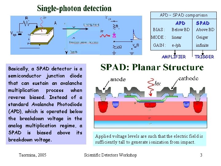
APD – SPAD comparison APD BIAS : Below BD Above BD MODE : linear Geiger GAIN : e-/ph infinite AMPLIFIER Basically, a SPAD detector is a semiconductor junction diode that can sustain an avalanche multiplication process when reverse biased. Instead of a standard Avalanche Photodiode (APD), which is operated below the breakdown voltage in the analog multiplication regime, a SPAD is biased above its breakdown voltage. Taormina, 2005 SPAD TRIGGER Applied voltage levels are such that the electric field is sufficiently tall to generate ionization from impact. Scientific Detectors Workshop 3

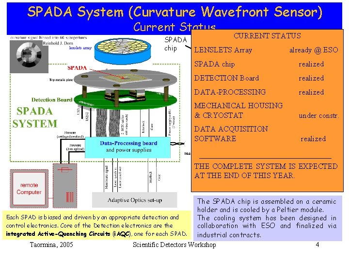
SPADA System (Curvature Wavefront Sensor) Current Status SPADA chip CURRENT STATUS LENSLETS Array SPADA chip MOREalready DETAILS @ ESO ON THE POSTER DETECTION Board realized SPADA realized element DATA-PROCESSING realized MECHANICAL HOUSING & CRYOSTAT under constr. DATA ACQUISITION SOFTWARE realized THE COMPLETE SYSTEM IS EXPECTED AT THE END OF THIS YEAR. The SPADA chip is assembled on a ceramic holder and is cooled by a Peltier module. Each SPAD is biased and driven by an appropriate detection and The cooling system has been designed in control electronics. Core of the Detection electronics are the collaboration with ESO and finalized via integrated Active-Quenching Circuits (i. AQC), one for each SPAD. industrial contracts. Taormina, 2005 Scientific Detectors Workshop 4

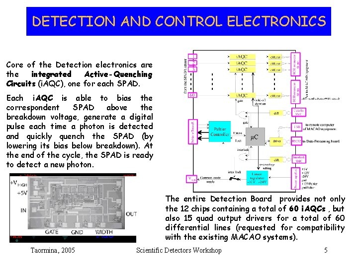
DETECTION AND CONTROL ELECTRONICS Core of the Detection electronics are the integrated Active-Quenching Circuits (i. AQC), one for each SPAD. Each i. AQC is able to bias the correspondent SPAD above the breakdown voltage, generate a digital pulse each time a photon is detected and quickly quench the SPAD (by lowering its bias below breakdown). At the end of the cycle, the SPAD is ready to detect a new photon. The entire Detection Board provides not only the 12 chips containing a total of 60 i. AQCs , but also 15 quad output drivers for a total of 60 differential lines (requested for compatibility with the existing MACAO systems). Taormina, 2005 Scientific Detectors Workshop 5

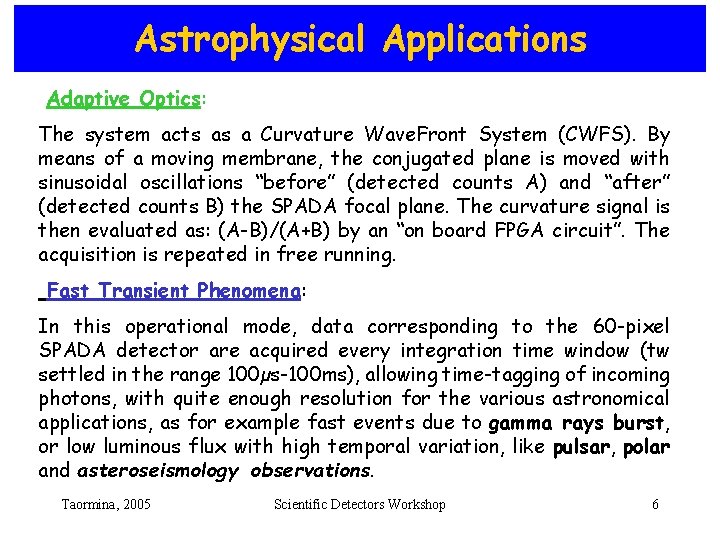
Astrophysical Applications Adaptive Optics: The system acts as a Curvature Wave. Front System (CWFS). By means of a moving membrane, the conjugated plane is moved with sinusoidal oscillations “before” (detected counts A) and “after” (detected counts B) the SPADA focal plane. The curvature signal is then evaluated as: (A-B)/(A+B) by an “on board FPGA circuit”. The acquisition is repeated in free running. Fast Transient Phenomena: In this operational mode, data corresponding to the 60 -pixel SPADA detector are acquired every integration time window (tw settled in the range 100µs-100 ms), allowing time-tagging of incoming photons, with quite enough resolution for the various astronomical applications, as for example fast events due to gamma rays burst, or low luminous flux with high temporal variation, like pulsar, polar and asteroseismology observations. Taormina, 2005 Scientific Detectors Workshop 6

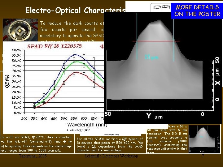
MORE DETAILS Electro-Optical Characteristics of a SPAD ON THE POSTER To reduce the dark counts at few counts per second, is mandatory to operate the SPAD at temperatures below 0 °C. MASK OF DIFFERENT Optical DIAMETER SINGLE SPAD Fiber Manufactured by STM A mechanical housing working under vacuum conditions hosts the packaged detector and can be easily interfaced with the measurement apparatus. Dark counts and after-pulsing The dark rate may be affected by after-pulsing traps in Si (releasing of charge at different time). In a 20 µm SPAD, @ 25°C, dark is constant vs the hold-off (switched-off) time no after-pulsing. Dark depends on the overvoltage and ranges from 300 to 1500 counts/s. Taormina, 2005 Quantum Efficiency QE measurements have been carried-out on 10, 20, 50 µm SPADs at overvoltages of: 10, 20 and 30 %. For all the SPADs we find a QE typical of Si devices that peaks at 550 -600 nm. We found a QE dependence from the SPAD diameter and the overvoltage. Scientific Detectors Workshop Response Uniformity The response uniformity has been measured by using a recently available facility constituted by a three axes translator that mount on top a reflective objective illuminated by a 10 µm pin-hole through a fiber optic that pick-up the monochromatic light from the Char. Sys. At each movement the corresponding count rate is acquired and stored in a file. Simultaneously an IDL procedure read the file and produces a 3 D plot of the currently acquired data. The 3 D plot shows a 50 x 50 µm scan with 5 µm resolution. The 5 X 5 µm central area presents a flat response (5000 counts/s), confirming the response uniformity in that area. 7

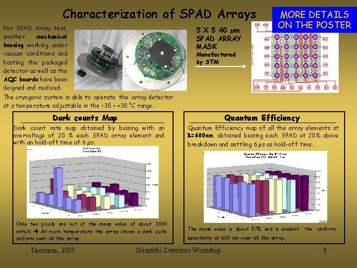
Characterization of SPAD Arrays For SPAD Array test, another mechanical housing working under vacuum conditions and hosting the packaged detector as well as the AQC boards have been deigned and realized. 5 X 5 40 µm SPAD ARRAY MASK MORE DETAILS ON THE POSTER Manufactured by STM The cryogenic system is able to operate the array detector at a temperature adjustable in the -30 ÷ +30 °C range. Dark counts Map Quantum Efficiency Dark count rate map obtained by biasing with an overvoltage of 20 % each SPAD array element and with an hold-off time of 6 µs. Quantum Efficiency map of all the array elements at =600 nm, obtained biasing each SPAD at 20% above breakdown and settling 6 µs as hold-off time. Quantum Efficiency Map @ 600 nm Overvoltage 20% hold-off 6 µs Only two pixels are out of the mean value of about 3000 cnts/s At room temperature the array shows a dark quite uniform over all the array. Taormina, 2005 The mean value is about 57% and is evident the uniform sensitivity at 600 nm over all the array. Scientific Detectors Workshop 8

Thank you For your attention/patience Taormina, 2005 Scientific Detectors Workshop 9