
Next generation 3 D digital Si PM for


- Slides: 24
Next generation 3 D digital Si. PM for precise timing resolution Jean-François Pratte F Nolet, W. Lemaire, F. Dubois, N. Roy, S. G. Carrier, A. Samson, G. St-Hilaire, S. A. Charlebois, R. Fontaine Interdisciplinary Institute for Technological Innovation (3 IT), Université de Sherbrooke 14 th Frontier Detectors for Frontier Physics 2018
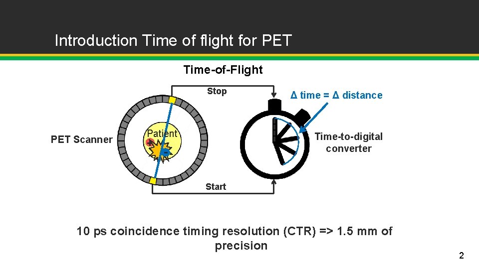
Introduction Time of flight for PET Time-of-Flight Stop PET Scanner Patient + Δ time = Δ distance Time-to-digital converter Start 10 ps coincidence timing resolution (CTR) => 1. 5 mm of precision 2
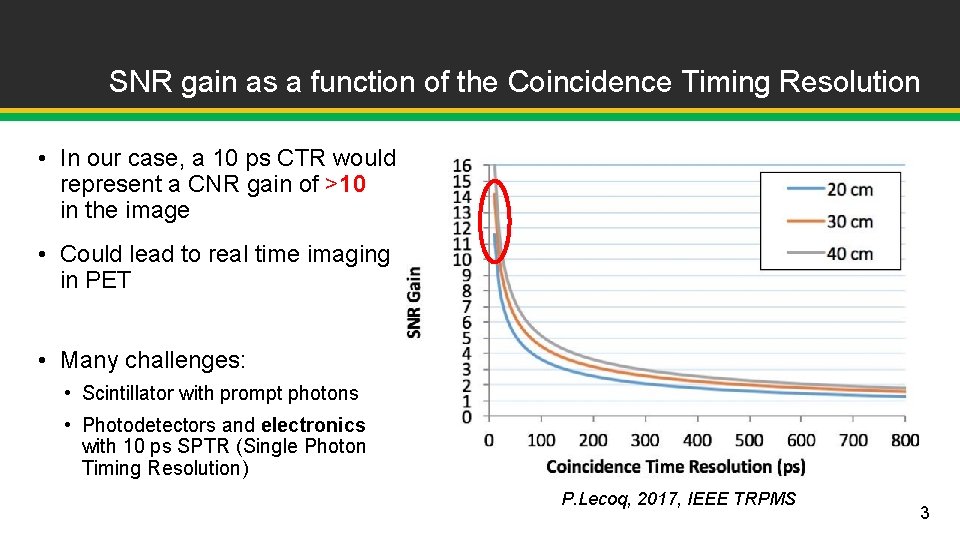
SNR gain as a function of the Coincidence Timing Resolution • In our case, a 10 ps CTR would represent a CNR gain of >10 in the image • Could lead to real time imaging in PET • Many challenges: • Scintillator with prompt photons • Photodetectors and electronics with 10 ps SPTR (Single Photon Timing Resolution) P. Lecoq, 2017, IEEE TRPMS 3
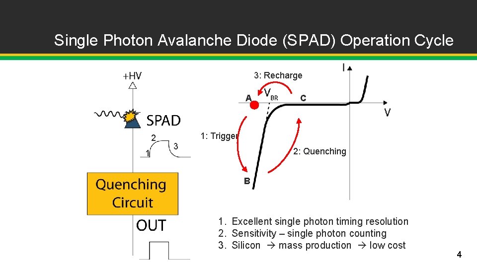
Single Photon Avalanche Diode (SPAD) Operation Cycle 3: Recharge A 2 1 C 1: Trigger 3 2: Quenching B 1. Excellent single photon timing resolution 2. Sensitivity – single photon counting 3. Silicon mass production low cost 4
Analog Versus Digital Si. PM… a Paradigm Shift… Bottom line, with an analog Si. PM we sum binary detectors (an array of SPAD) to get a linear response… Then, use a current/transimpedance amplifier + shaper + ADC to digitize the data… again! • How to take advantage of the SPAD’s digital nature? • Can power consumption be saved using a digital approach compared to the classic analog readout dealing with large input capacitance of the serial / parallel connections of Si. PM? jean-francois. pratte@usherbrooke. ca 5
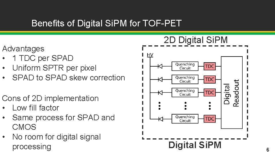
Benefits of Digital Si. PM for TOF-PET Advantages • 1 TDC per SPAD • Uniform SPTR per pixel • SPAD to SPAD skew correction Cons of 2 D implementation • Low fill factor • Same process for SPAD and CMOS • No room for digital signal processing 2 D Digital Si. PM 6
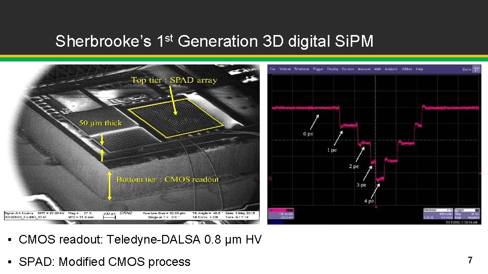
Sherbrooke’s 1 st Generation 3 D digital Si. PM • CMOS readout: Teledyne-DALSA 0. 8 µm HV • SPAD: Modified CMOS process 7
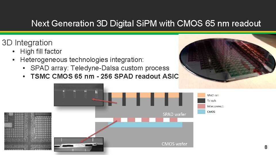
Next Generation 3 D Digital Si. PM with CMOS 65 nm readout 3 D Integration • High fill factor • Heterogeneous technologies integration: • SPAD array: Teledyne-Dalsa custom process • TSMC CMOS 65 nm - 256 SPAD readout ASIC 8
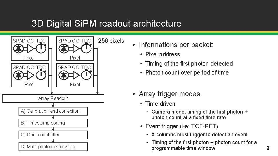
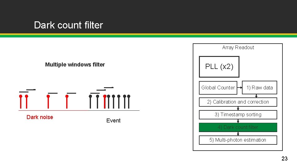
3 D Digital Si. PM readout architecture SPAD QC TDC Pixel SPAD QC TDC Pixel 256 pixels • Informations per packet: • Pixel address • Timing of the first photon detected • Photon count over period of time Pixel Array Readout A) Calibration and correction B) Timestamp sorting C) Dark count filter D) Multi-photon estimation • Array trigger modes: • Time driven • Camera mode: timing of the first photon + photon count at a fixed time rate • Event trigger (i-e: TOF-PET) • X columns must trigger to detect an event • Timing of the first photon + photon count for a programmable time window 9
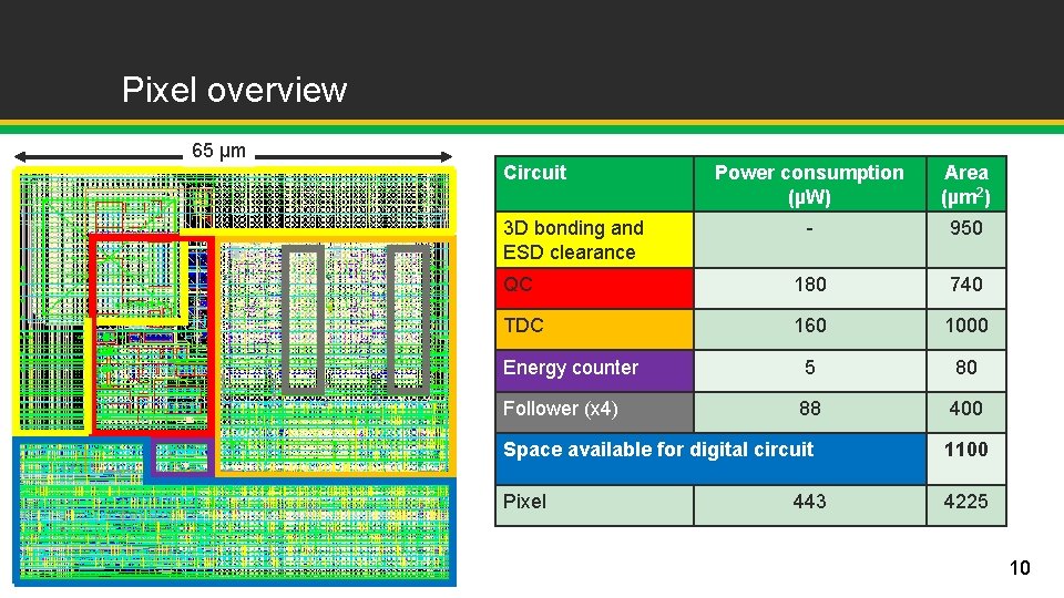
Pixel overview 65 µm Circuit Power consumption (µW) Area (µm 2) - 950 QC 180 740 TDC 160 1000 Energy counter 5 80 Follower (x 4) 88 400 3 D bonding and ESD clearance Space available for digital circuit 1100 Pixel 4225 443 10
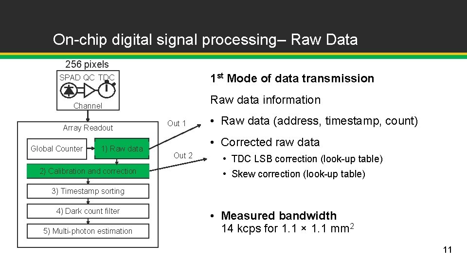
On-chip digital signal processing– Raw Data 256 pixels 1 st Mode of data transmission SPAD QC TDC Raw data information Channel Array Readout Global Counter 1) Raw data 2) Calibration and correction Out 1 • Raw data (address, timestamp, count) • Corrected raw data Out 2 • TDC LSB correction (look-up table) • Skew correction (look-up table) 3) Timestamp sorting 4) Dark count filter 5) Multi-photon estimation • Measured bandwidth 14 kcps for 1. 1 × 1. 1 mm 2 11
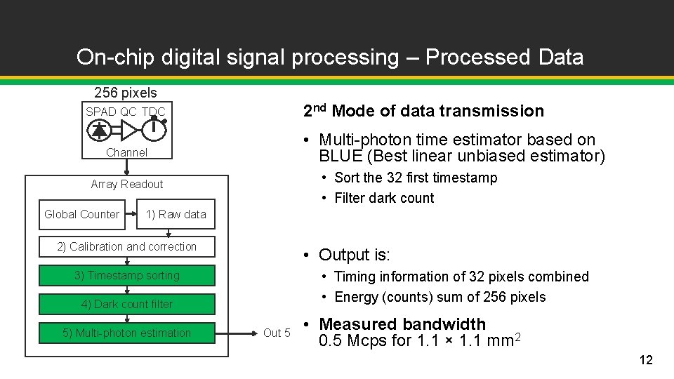
On-chip digital signal processing – Processed Data 256 pixels 2 nd Mode of data transmission SPAD QC TDC • Multi-photon time estimator based on BLUE (Best linear unbiased estimator) Channel • Sort the 32 first timestamp • Filter dark count Array Readout Global Counter 1) Raw data 2) Calibration and correction • Output is: • Timing information of 32 pixels combined • Energy (counts) sum of 256 pixels 3) Timestamp sorting 4) Dark count filter 5) Multi-photon estimation Out 5 • Measured bandwidth 0. 5 Mcps for 1. 1 × 1. 1 mm 2 12
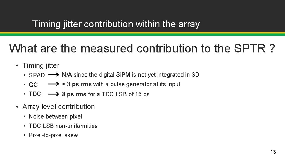
Timing jitter contribution within the array What are the measured contribution to the SPTR ? • Timing jitter • SPAD N/A since the digital Si. PM is not yet integrated in 3 D • QC < 3 ps rms with a pulse generator at its input • TDC 8 ps rms for a TDC LSB of 15 ps • Array level contribution • Noise between pixel • TDC LSB non-uniformities • Pixel-to-pixel skew 13
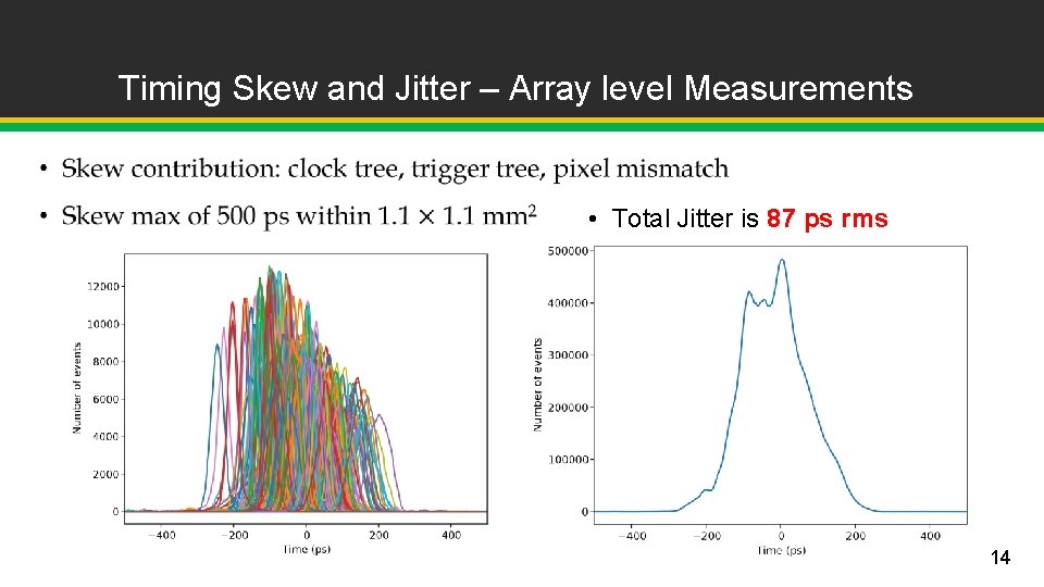
Timing Skew and Jitter – Array level Measurements • • Total Jitter is 87 ps rms 14
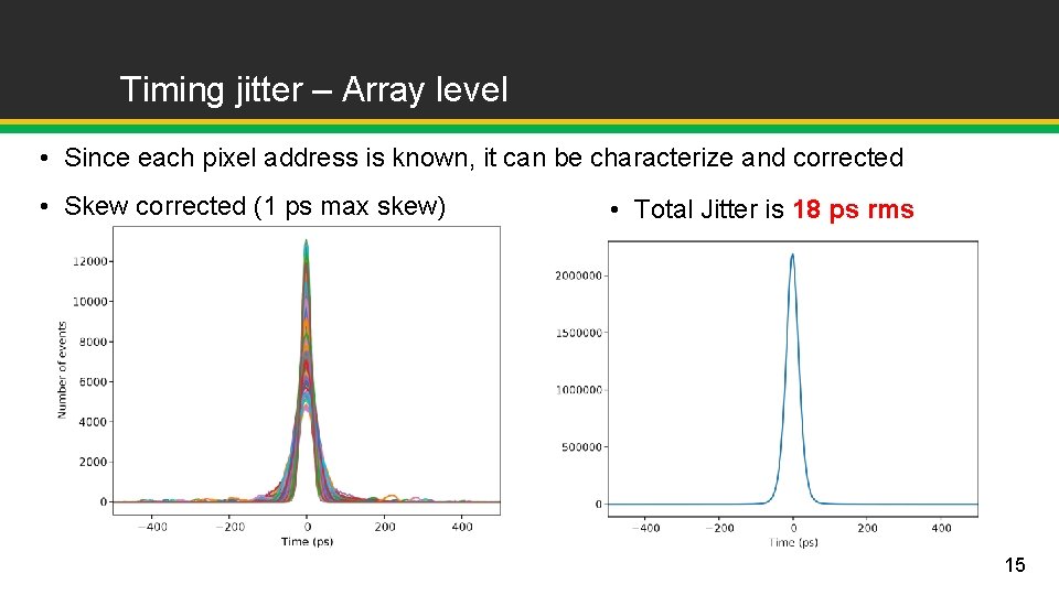
Timing jitter – Array level • Since each pixel address is known, it can be characterize and corrected • Skew corrected (1 ps max skew) • Total Jitter is 18 ps rms 15
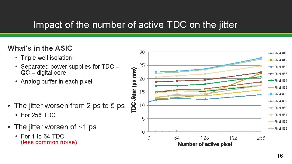
Impact of the number of active TDC on the jitter What’s in the ASIC • The jitter worsen from 2 ps to 5 ps • For 256 TDC • The jitter worsen of ~1 ps • For 1 to 64 TDC (less common noise) Pixel #48 Pixel #49 TDC Jitter (ps rms) • Triple well isolation • Separated power supplies for TDC – QC – digital core • Analog buffer in each pixel 30 25 Pixel #52 Pixel #53 20 Pixel #54 Pixel #56 15 Pixel #58 Pixel #59 10 Pixel #61 5 Pixel #62 Pixel #63 0 0 64 128 192 256 Number of active pixel 16
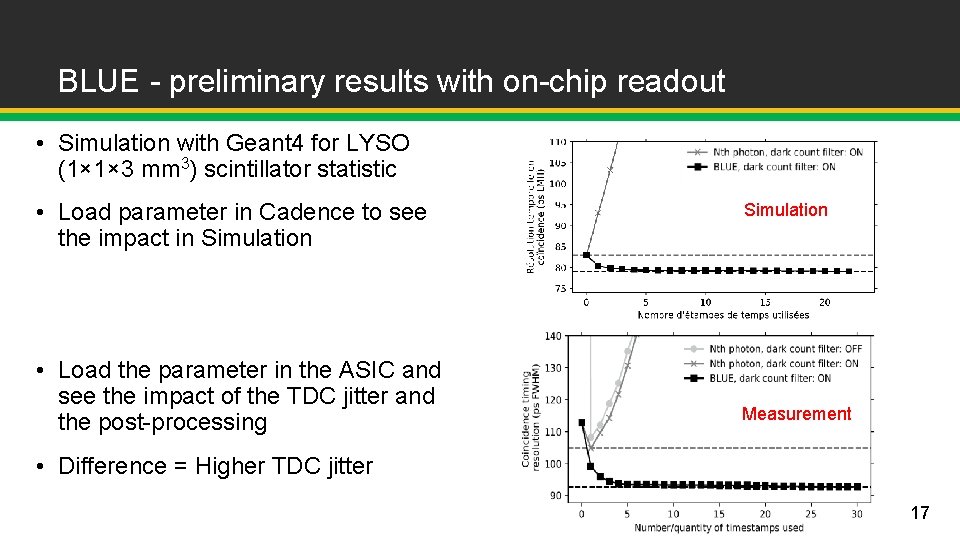
BLUE - preliminary results with on-chip readout • Simulation with Geant 4 for LYSO (1× 1× 3 mm 3) scintillator statistic • Load parameter in Cadence to see the impact in Simulation • Load the parameter in the ASIC and see the impact of the TDC jitter and the post-processing Simulation Measurement • Difference = Higher TDC jitter 17
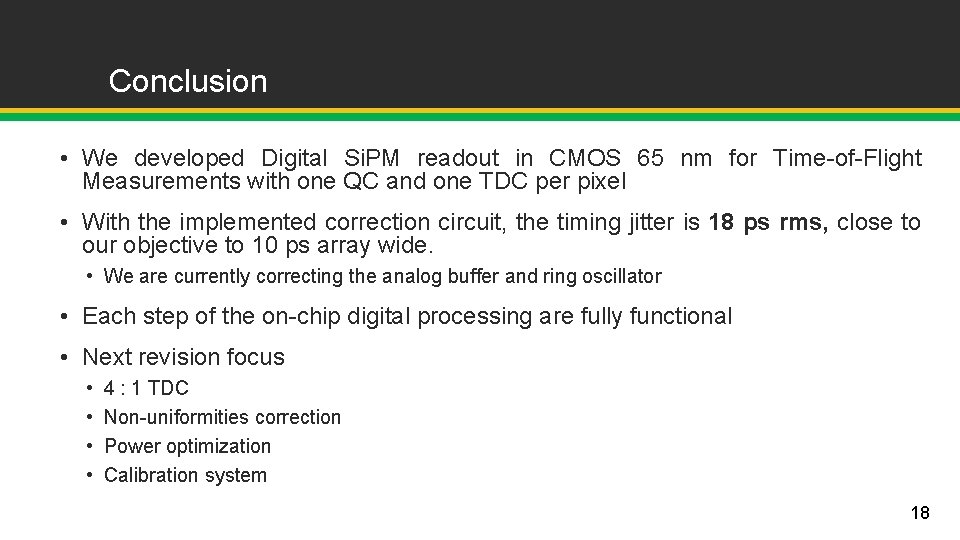
Conclusion • We developed Digital Si. PM readout in CMOS 65 nm for Time-of-Flight Measurements with one QC and one TDC per pixel • With the implemented correction circuit, the timing jitter is 18 ps rms, close to our objective to 10 ps array wide. • We are currently correcting the analog buffer and ring oscillator • Each step of the on-chip digital processing are fully functional • Next revision focus • • 4 : 1 TDC Non-uniformities correction Power optimization Calibration system 18
Conclusion • 3 D digital Si. PM is a versatile technology. • A 3 D digital Si. PM is currently under development for LAr and LXe experiments • We are member of the n. EXO collaboration for double beta decays neutrinoless • Next generation hundred tons LAr 19
Acknowledgements • Thank you for your attention 20
Back-up slides 21
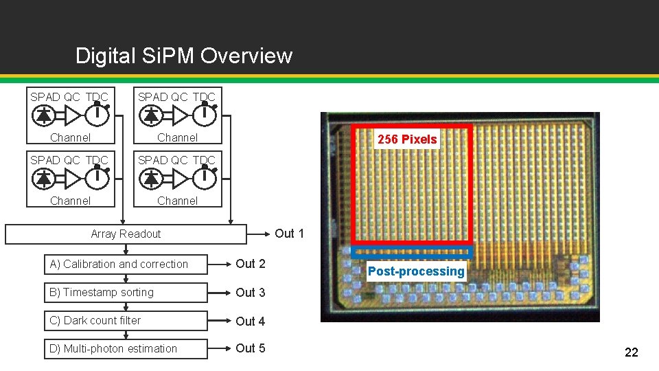
Digital Si. PM Overview SPAD QC TDC Channel SPAD QC TDC Channel 256 Pixels Channel Out 1 Array Readout A) Calibration and correction Out 2 B) Timestamp sorting Out 3 C) Dark count filter Out 4 D) Multi-photon estimation Out 5 Post-processing 22
Dark count filter Array Readout Multiple windows filter PLL (x 2) Global Counter 1) Raw data 2) Calibration and correction Dark noise 3) Timestamp sorting Event 4) Dark count filter 5) Multi-photon estimation 23
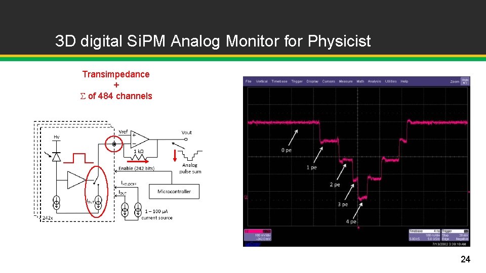
3 D digital Si. PM Analog Monitor for Physicist Transimpedance + of 484 channels 24