SDD Status N Zampa INFN Trieste WFM Meeting

![Test plan Step F 200 ke. V [p·cm-2] F 800 ke. V [p·cm-2] Expected Test plan Step F 200 ke. V [p·cm-2] F 800 ke. V [p·cm-2] Expected](https://slidetodoc.com/presentation_image_h2/c693c7a44f904009c4819e551c4ebd15/image-4.jpg)


- Slides: 30

SDD Status N. Zampa – INFN Trieste WFM Meeting @ DTU Space October 24 th, 2012

Summary • • October 24 th, 2012 Soft Protons Test Debris Test Hygroscopy Test Third Prototype Run (XDXL-2) Detector Efficiency Interfaces Vacuum Considerations 2

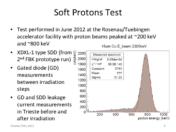
Soft Protons Test • Test performed in June 2012 at the Rosenau/Tuebingen accelerator facility with proton beams peaked at ~200 ke. V and ~800 ke. V • XDXL-1 type SDD (from 2 nd FBK prototype run) • Gated diode (GD) measurements between irradiation steps • GD and SDD leakage current measurements in Trieste before and after irradiation October 24 th, 2012 3
![Test plan Step F 200 ke V pcm2 F 800 ke V pcm2 Expected Test plan Step F 200 ke. V [p·cm-2] F 800 ke. V [p·cm-2] Expected](https://slidetodoc.com/presentation_image_h2/c693c7a44f904009c4819e551c4ebd15/image-4.jpg)
Test plan Step F 200 ke. V [p·cm-2] F 800 ke. V [p·cm-2] Expected integrated damage TID [rad(Si. O 2)] ΔIleak [p. A] LAD WFM 1 3. 50· 106 7. 85· 105 34. 4 16. 3 2. 4 2 3. 50· 106 7. 85· 105 68. 7 32. 6 4. 9 3 0 2. 40· 107 155. 4 195. 9 29. 3 4 1. 10· 105 4. 28· 107 310. 7 486. 7 72. 7 LAD: 4. 5 x WFM: 2 x 14. 9 x 2 x wrt LOFT • The proton fluence at the two energies was estimated considering a worst case of 5 years mission duration with LOFT always oriented towards the maximum of the particle flux • Anode pitches in the SDD are different from the LOFT design values: the currents should be scaled accordingly to get the correct damage from the measurements (~0. 5 x for WFM) October 24 th, 2012 4

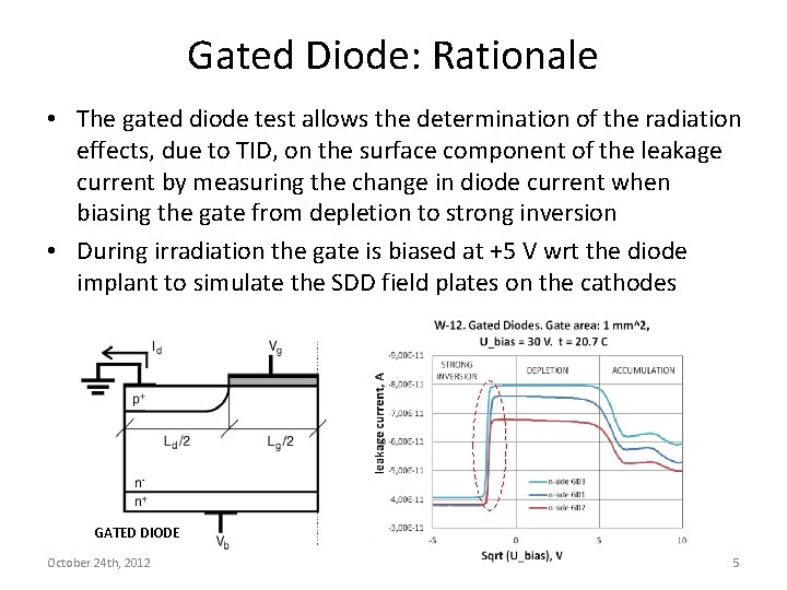
Gated Diode: Rationale • The gated diode test allows the determination of the radiation effects, due to TID, on the surface component of the leakage current by measuring the change in diode current when biasing the gate from depletion to strong inversion • During irradiation the gate is biased at +5 V wrt the diode implant to simulate the SDD field plates on the cathodes GATED DIODE October 24 th, 2012 5

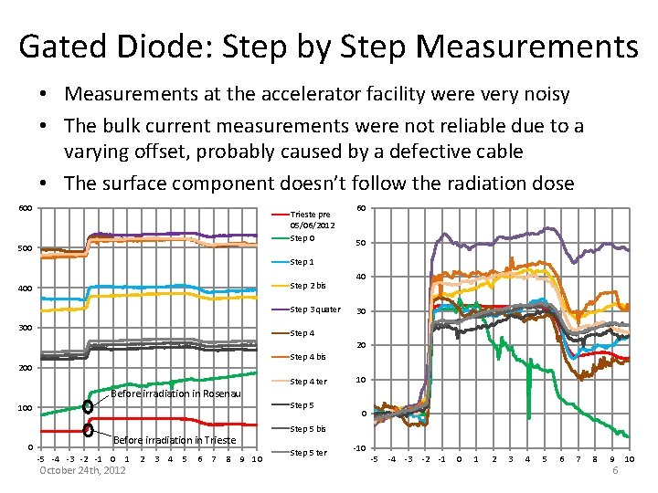
Gated Diode: Step by Step Measurements • Measurements at the accelerator facility were very noisy • The bulk current measurements were not reliable due to a varying offset, probably caused by a defective cable • The surface component doesn’t follow the radiation dose 600 Trieste pre 05/06/2012 Step 0 500 60 50 Step 1 Step 2 bis 400 Step 3 quater 300 40 30 Step 4 20 Step 4 bis 200 Step 4 ter Before irradiation in Rosenau 100 0 1 October 24 th, 2012 2 3 4 5 6 7 8 0 Step 5 bis Before irradiation in Trieste -5 -4 -3 -2 -1 0 Step 5 10 9 10 Step 5 ter -10 -5 -4 -3 -2 -1 0 1 2 3 4 5 6 7 8 9 6 10

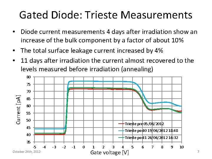
Gated Diode: Trieste Measurements • Diode current measurements 4 days after irradiation show an increase of the bulk component by a factor of about 10% • The total surface leakage current increased by 4% • 11 days after irradiation the current almost recovered to the levels measured before irradiation (annealing) 80 75 Current [p. A] 70 65 60 55 50 Trieste pre 05/06/2012 45 Trieste post 0 19/06/2012 18: 48 40 Trieste post 1 26/06/2012 16: 32 35 -5 October 24 th, 2012 -4 -3 -2 -1 0 1 2 3 4 Gate voltage [V] 5 6 7 8 9 10 7

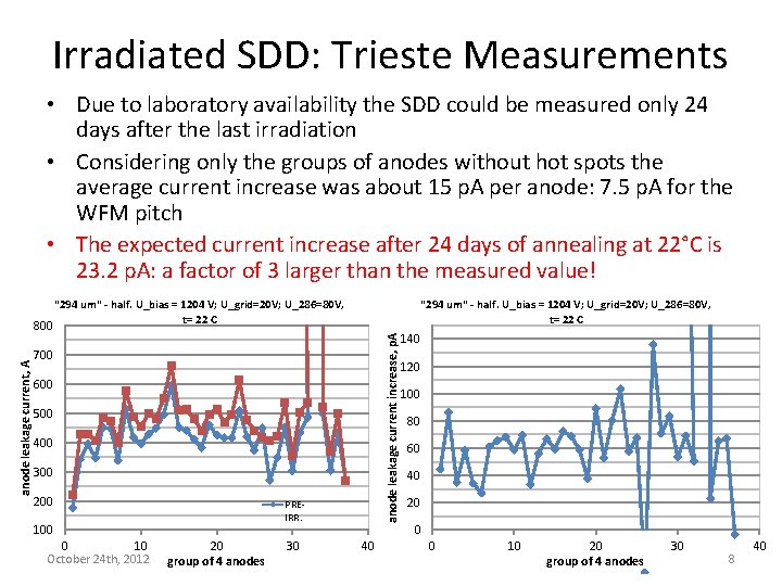
Irradiated SDD: Trieste Measurements • Due to laboratory availability the SDD could be measured only 24 days after the last irradiation • Considering only the groups of anodes without hot spots the average current increase was about 15 p. A per anode: 7. 5 p. A for the WFM pitch • The expected current increase after 24 days of annealing at 22°C is 23. 2 p. A: a factor of 3 larger than the measured value! "294 um" - half. U_bias = 1204 V; U_grid=20 V; U_286=80 V, t= 22 C anode leakage current increase, p. A anode leakage current, A 800 "294 um" - half. U_bias = 1204 V; U_grid=20 V; U_286=80 V, t= 22 C 700 600 500 400 300 200 PREIRR. 100 0 10 October 24 th, 2012 20 group of 4 anodes 30 40 120 100 80 60 40 20 0 0 10 20 group of 4 anodes 30 8 40

Soft Protons: Conclusions • The test results are not consistent with the expectations • The damage calculations and the beam parameters (energy, flux) have been checked and seem to be correct • In principle, a high detector temperature during the transport back to Trieste could have increased the annealing rate, but the discrepancy could be explained only if the detector was subject, for example, to a temperature of ~40°C for 2 days! • To exclude the possibility of undiscovered experimental errors in the June test a new one will be carried out in the second half of November 2012, increasing the fluence with a beam energy of 800 ke. V (expected damage higher by a factor of 5) • This time the SDD will be measured at earlier times after irradiation and the annealing rate will be verified in an extended time interval October 24 th, 2012 9

Debris test • Investigation of the damage produced to the SDD by the impact of dust particles in orbit • A preliminary estimation of debris and micrometeoroid fluxes on LOFT orbit performed with ORDEM 2000 has shown that the most threatening particles are debris of size 1 μm • From ESA ECSS-E-ST-10 -04 C the average velocity is 10 km/s, the particles have a spherical shape, and density 2. 8 g/cm 3 (Al, 2. 7 g/cm 3, is a good approximation) • The penetration depth of 1 μm Al particles with velocity 10 km/s is estimated to be about 2. 5 μm • Test performed at the Dust Accelerator Facility of the Max. Plank Institut für Kernphysik in Heidelberg with olivine (3. 3 g/cm 3, (Mg, Fe)2 Si. O 4) particles of different sizes and velocities October 24 th, 2012 10

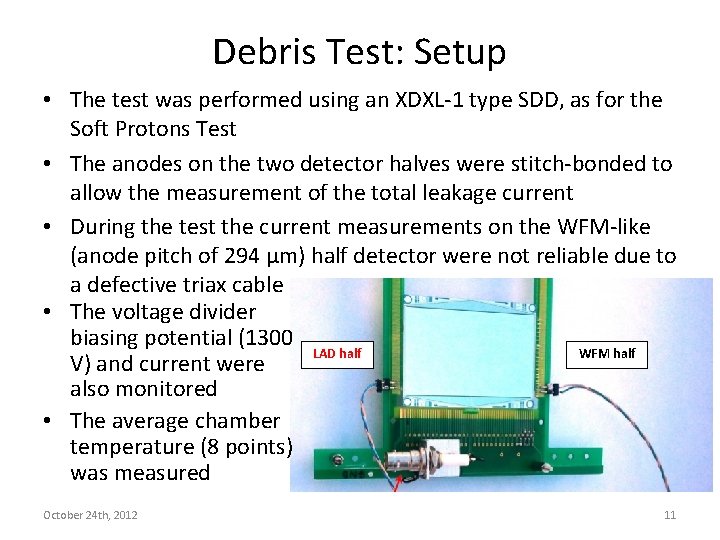
Debris Test: Setup • The test was performed using an XDXL-1 type SDD, as for the Soft Protons Test • The anodes on the two detector halves were stitch-bonded to allow the measurement of the total leakage current • During the test the current measurements on the WFM-like (anode pitch of 294 μm) half detector were not reliable due to a defective triax cable • The voltage divider biasing potential (1300 LAD half WFM half V) and current were also monitored • The average chamber temperature (8 points) was measured October 24 th, 2012 11

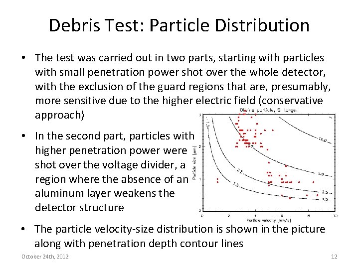
Debris Test: Particle Distribution • The test was carried out in two parts, starting with particles with small penetration power shot over the whole detector, with the exclusion of the guard regions that are, presumably, more sensitive due to the higher electric field (conservative approach) • In the second part, particles with higher penetration power were shot over the voltage divider, a region where the absence of an aluminum layer weakens the detector structure • The particle velocity-size distribution is shown in the picture along with penetration depth contour lines October 24 th, 2012 12

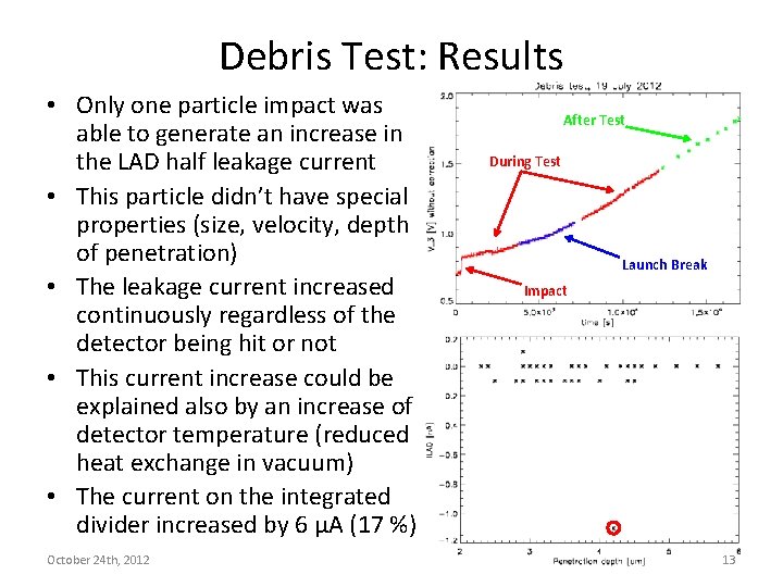
Debris Test: Results • Only one particle impact was able to generate an increase in the LAD half leakage current • This particle didn’t have special properties (size, velocity, depth of penetration) • The leakage current increased continuously regardless of the detector being hit or not • This current increase could be explained also by an increase of detector temperature (reduced heat exchange in vacuum) • The current on the integrated divider increased by 6 μA (17 %) October 24 th, 2012 After Test During Test Launch Break Impact 13

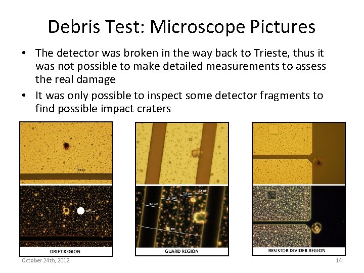
Debris Test: Microscope Pictures • The detector was broken in the way back to Trieste, thus it was not possible to make detailed measurements to assess the real damage • It was only possible to inspect some detector fragments to find possible impact craters October 24 th, 2012 14

Debris Test: Conclusions • The SDD seems to be quite robust, at least for impact energies in the range explored • Only one particle out of 73 with penetration depth > 2. 5 μm was able to damage the detector in a measurable way • In the next test the actual detector temperature should be measured, and the leakage current should be monitored in vacuum for a long time, without shooting particles, to understand thermal stability of the SDD • The ORDEM 2000(NASA) model is valid only for particles with a diameter larger than 10 μm. The MASTER 2005(ESA) model is valid down to 1 μm: a preliminary analysis has shown that our ORDEM 2000 estimate of the flux of 1 μm debris is overestimated by an order of magnitude so that micro-meteoroids could be more abundant. This question will be investigated in the near future, and a test with iron particles will be planned if necessary October 24 th, 2012 15

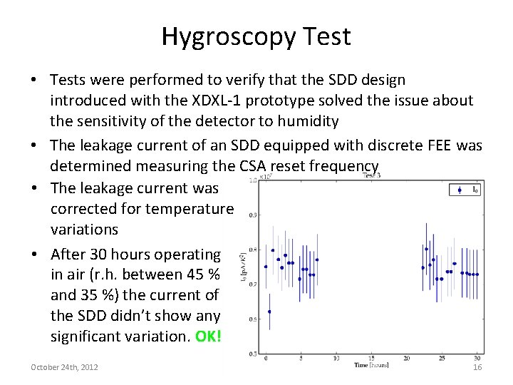
Hygroscopy Test • Tests were performed to verify that the SDD design introduced with the XDXL-1 prototype solved the issue about the sensitivity of the detector to humidity • The leakage current of an SDD equipped with discrete FEE was determined measuring the CSA reset frequency • The leakage current was corrected for temperature variations • After 30 hours operating in air (r. h. between 45 % and 35 %) the current of the SDD didn’t show any significant variation. OK! October 24 th, 2012 16

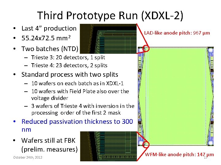
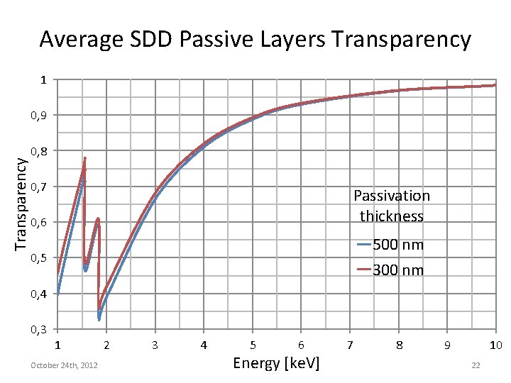
Third Prototype Run (XDXL-2) • Last 4” production • 55. 24 x 72. 5 mm 2 • Two batches (NTD) LAD-like anode pitch: 967 μm – Trieste 3: 20 detectors, 1 split – Trieste 4: 23 detectors, 2 splits • Standard process with two splits – 10 wafers on each batch as in XDXL-1 – 10 wafers with Field Plate also over the voltage divider – 3 wafers of Trieste 4 with inversion in the processing order of the first 2 mask • Reduced passivation thickness to 300 nm • Wafers still at FBK (prelim. measures) October 24 th, 2012 WFM-like anode pitch: 14717μm

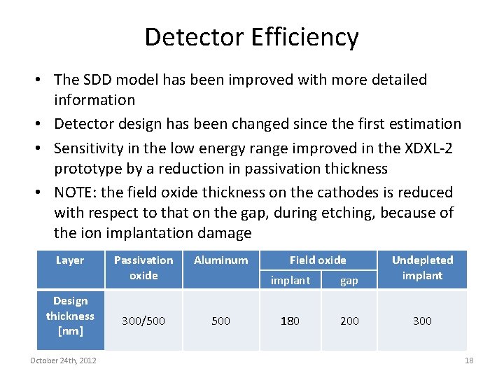
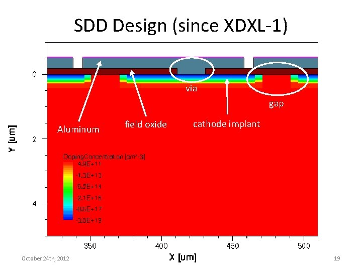
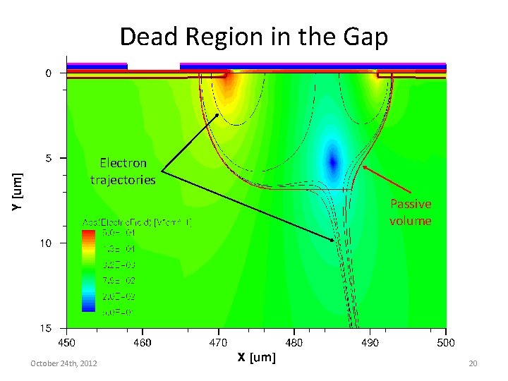
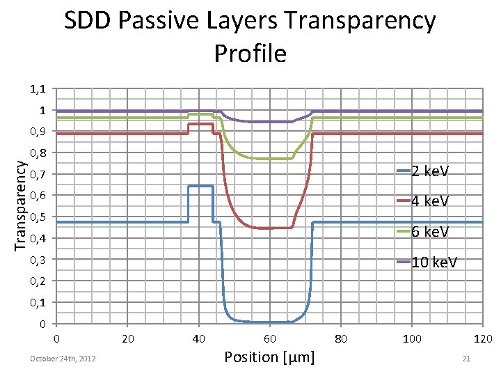
Detector Efficiency • The SDD model has been improved with more detailed information • Detector design has been changed since the first estimation • Sensitivity in the low energy range improved in the XDXL-2 prototype by a reduction in passivation thickness • NOTE: the field oxide thickness on the cathodes is reduced with respect to that on the gap, during etching, because of the ion implantation damage Layer Design thickness [nm] October 24 th, 2012 Passivation oxide Aluminum 300/500 Field oxide implant gap Undepleted implant 180 200 300 18

SDD Design (since XDXL-1) via gap Aluminum October 24 th, 2012 field oxide cathode implant 19

Dead Region in the Gap Electron trajectories Passive volume October 24 th, 2012 20

SDD Passive Layers Transparency Profile 1, 1 1 0, 9 Transparency 0, 8 0, 7 2 ke. V 0, 6 4 ke. V 0, 5 0, 4 6 ke. V 0, 3 10 ke. V 0, 2 0, 1 0 0 October 24 th, 2012 20 40 60 Position [μm] 80 100 120 21

Average SDD Passive Layers Transparency 1 Transparency 0, 9 0, 8 0, 7 Passivation thickness 0, 6 500 nm 300 nm 0, 5 0, 4 0, 3 1 October 24 th, 2012 2 3 4 5 6 Energy [ke. V] 7 8 9 10 22

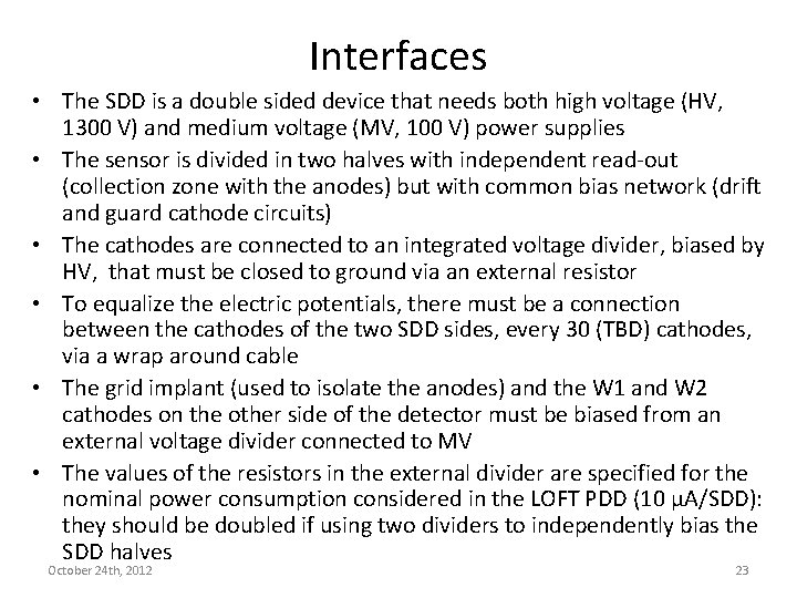
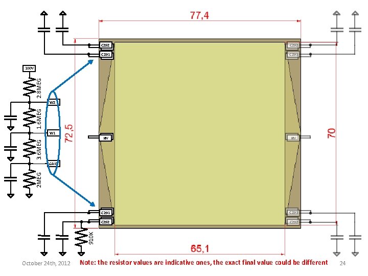
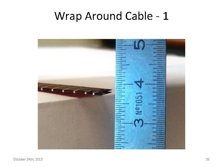
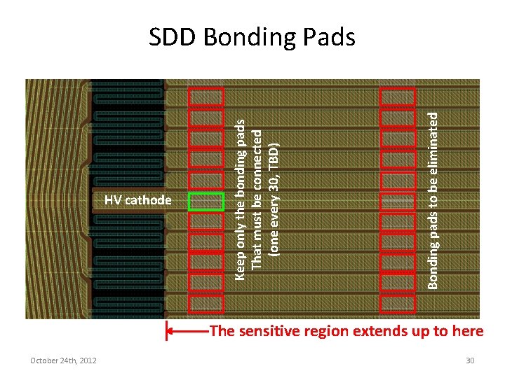
Interfaces • The SDD is a double sided device that needs both high voltage (HV, 1300 V) and medium voltage (MV, 100 V) power supplies • The sensor is divided in two halves with independent read-out (collection zone with the anodes) but with common bias network (drift and guard cathode circuits) • The cathodes are connected to an integrated voltage divider, biased by HV, that must be closed to ground via an external resistor • To equalize the electric potentials, there must be a connection between the cathodes of the two SDD sides, every 30 (TBD) cathodes, via a wrap around cable • The grid implant (used to isolate the anodes) and the W 1 and W 2 cathodes on the other side of the detector must be biased from an external voltage divider connected to MV • The values of the resistors in the external divider are specified for the nominal power consumption considered in the LOFT PDD (10 μA/SDD): they should be doubled if using two dividers to independently bias the SDD halves October 24 th, 2012 23

C 292 C 291 HV HV C 291 C 292 2. 8 MEG 100 V 1. 6 MEG W 2 3. 6 MEG W 1 910 K 2 MEG GRID October 24 th, 2012 Note: the resistor values are indicative ones, the exact final value could be different 24

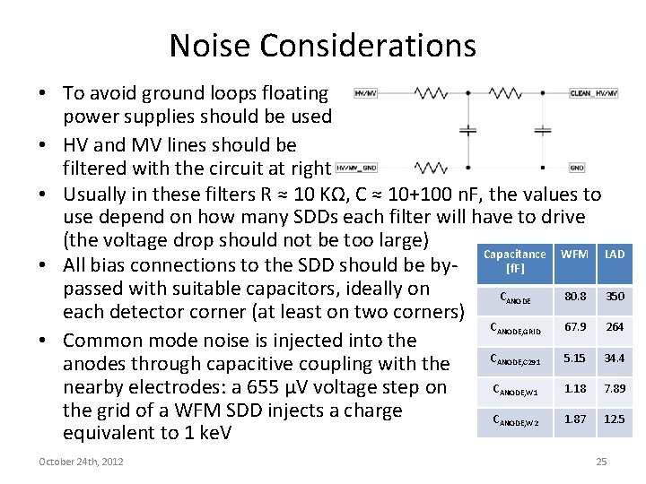
Noise Considerations • To avoid ground loops floating power supplies should be used • HV and MV lines should be filtered with the circuit at right • Usually in these filters R ≈ 10 KΩ, C ≈ 10+100 n. F, the values to use depend on how many SDDs each filter will have to drive (the voltage drop should not be too large) Capacitance WFM LAD • All bias connections to the SDD should be by[f. F] passed with suitable capacitors, ideally on C 80. 8 350 each detector corner (at least on two corners) C 67. 9 264 • Common mode noise is injected into the C 5. 15 34. 4 anodes through capacitive coupling with the C 1. 18 7. 89 nearby electrodes: a 655 μV voltage step on the grid of a WFM SDD injects a charge C 1. 87 12. 5 equivalent to 1 ke. V ANODE, GRID ANODE, C 291 ANODE, W 2 October 24 th, 2012 25

Wrap Around Cable - 1 October 24 th, 2012 26

Wrap Around Cable - 2 October 24 th, 2012 27

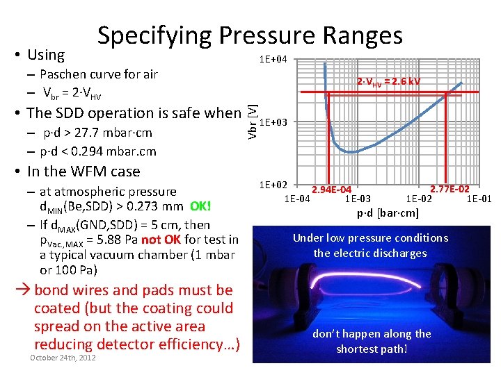
Vacuum Considerations • High voltage equipment should be designed to avoid electric discharges • For non potted devices the breakdown voltage depends on gas type and pressure, according to the appropriate Paschen curves (for uniform electric fields) • Safety margins should be enforced, particularly when the electric field is not uniform • For any equipment (geometry+electric field) a gas pressure range should be specified for its operation • Things get complicated when the equipment should work both at atmospheric pressure (e. g. in laboratory tests) and under vacuum or low pressureconditions (in space or laboratory) October 24 th, 2012 28

• Using Specifying Pressure Ranges 1 E+04 – Paschen curve for air – Vbr = 2·VHV – p·d > 27. 7 mbar·cm – p·d < 0. 294 mbar. cm • In the WFM case – at atmospheric pressure d. MIN(Be, SDD) > 0. 273 mm OK! – If d. MAX(GND, SDD) = 5 cm, then p. Vac. , MAX = 5. 88 Pa not OK for test in a typical vacuum chamber (1 mbar or 100 Pa) à bond wires and pads must be coated (but the coating could spread on the active area reducing detector efficiency…) October 24 th, 2012 Vbr [V] • The SDD operation is safe when 2·VHV = 2. 6 k. V 1 E+03 1 E+02 2. 94 E-04 1 E-03 2. 77 E-02 1 E-01 p·d [bar·cm] Under low pressure conditions the electric discharges don’t happen along the shortest path! 29

HV cathode October 24 th, 2012 Bonding pads to be eliminated Keep only the bonding pads That must be connected (one every 30, TBD) SDD Bonding Pads The sensitive region extends up to here 30