OnChip Inductance Extraction Concept Formulae 2002 3 Hyungsuk


- Slides: 22
On-Chip Inductance Extraction - Concept & Formulae – 2002. 3 Hyungsuk Kim hyungsuk@cae. wisc. edu
Out. Line n n n Introduction – On-Chip Inductance Loop Inductance and Partial Inductance Closed Forms of Inductance Formulae ü Self Inductance Formulae - Hoer, Fast. Henry, Ruehli, Grover ü Mutual Inductance Formulae - Hoer (Fast. Henry), Ruehli, Grover n n Computational Results Conclusion
Introduction – On-Chip Inductance n As the clock frequency grows fast, the reactance becomes larger for on-chip interconnections Z = R + jw. L ü w is determined not by clock frequency itself but by clock edge w ~ 1/(rising time) n More layers are applied, wider conductors are used ü n Wide conductor => low resistance Multiple layer interconnections make complex return loops ü Inductance is defined in the closed loop in EM
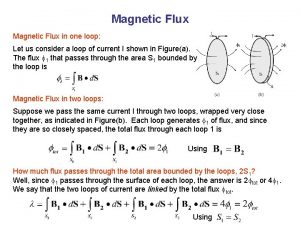
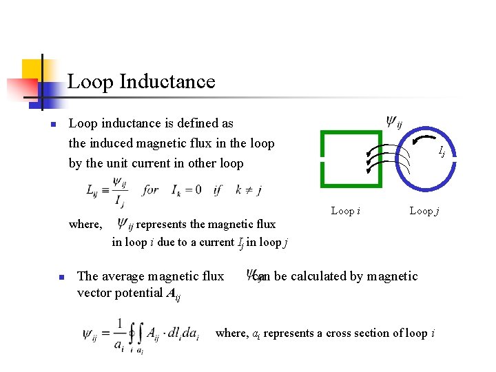
Loop Inductance Loop inductance is defined as the induced magnetic flux in the loop by the unit current in other loop n Ij Loop i where, n Loop j represents the magnetic flux in loop i due to a current Ij in loop j The average magnetic flux vector potential Aij can be calculated by magnetic where, ai represents a cross section of loop i
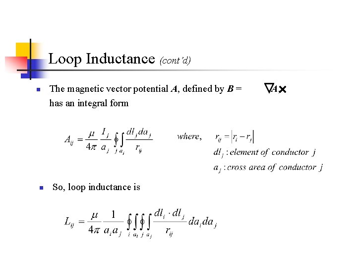
Loop Inductance (cont’d) n n The magnetic vector potential A, defined by B = has an integral form So, loop inductance is A,
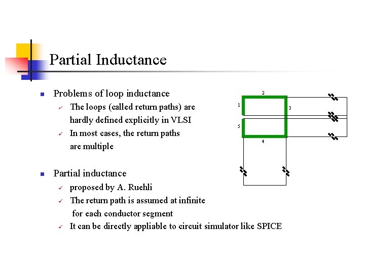
Partial Inductance n Problems of loop inductance ü ü n The loops (called return paths) are hardly defined explicitly in VLSI In most cases, the return paths are multiple 2 1 3 5 4 Partial inductance ü ü ü proposed by A. Ruehli The return path is assumed at infinite for each conductor segment It can be directly appliable to circuit simulator like SPICE
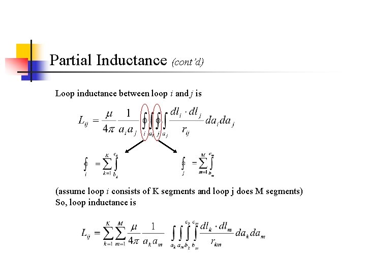
Partial Inductance (cont’d) Loop inductance between loop i and j is (assume loop i consists of K segments and loop j does M segments) So, loop inductance is
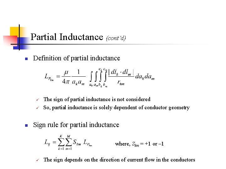
Partial Inductance (cont’d) n Definition of partial inductance ü ü n The sign of partial inductance is not considered So, partial inductance is solely dependent of conductor geometry Sign rule for partial inductance where, Skm = +1 or – 1 ü The sign depends on the direction of current flow in the conductors
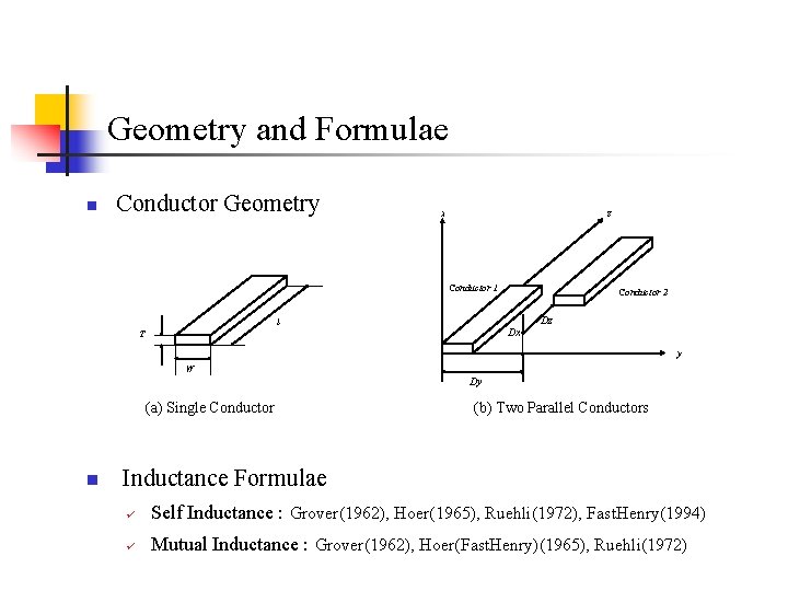
Geometry and Formulae n Conductor Geometry x z Conductor 1 Conductor 2 Dz l Dx T y W Dy (a) Single Conductor n (b) Two Parallel Conductors Inductance Formulae ü Self Inductance : Grover(1962), Hoer(1965), Ruehli(1972), Fast. Henry(1994) ü Mutual Inductance : Grover(1962), Hoer(Fast. Henry)(1965), Ruehli(1972)
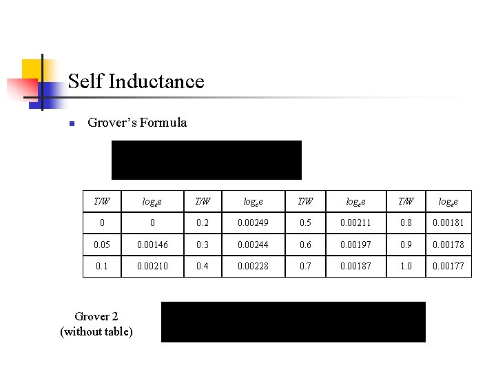
Self Inductance n Grover’s Formula T/W logee 0 0 0. 2 0. 00249 0. 5 0. 00211 0. 8 0. 00181 0. 05 0. 00146 0. 3 0. 00244 0. 6 0. 00197 0. 9 0. 00178 0. 1 0. 00210 0. 4 0. 00228 0. 7 0. 00187 1. 0 0. 00177 Grover 2 (without table)
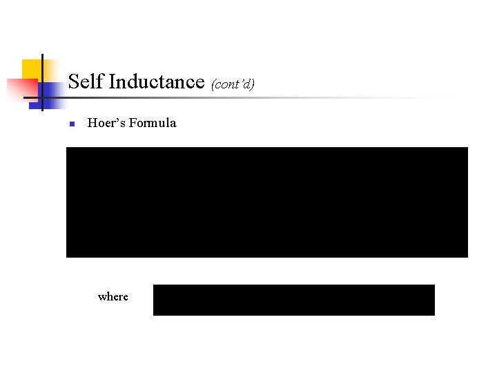
Self Inductance (cont’d) n Hoer’s Formula where
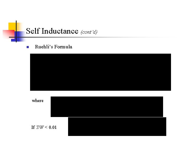
Self Inductance (cont’d) n Ruehli’s Formula where If T/W < 0. 01
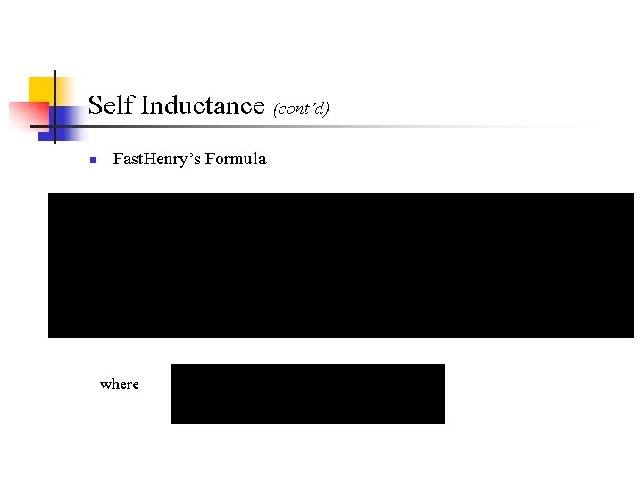
Self Inductance (cont’d) n Fast. Henry’s Formula where
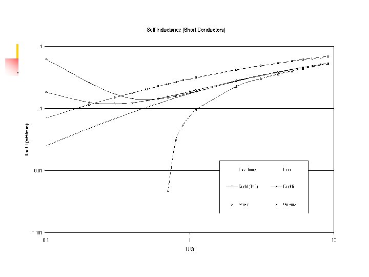
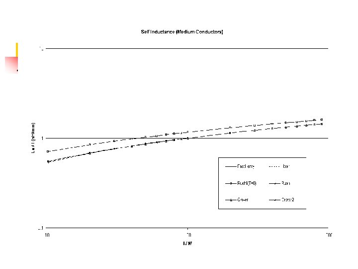
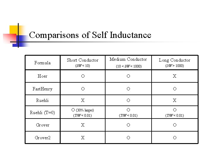
Comparisons of Self Inductance Short Conductor Medium Conductor Long Conductor (l/W < 10) (10 < l/W < 1000) (l/W > 1000) Hoer O O X Fast. Henry O O O Ruehli X O (30% larger) O O (T/W < 0. 01) Grover X O O Grover 2 X O O Formula Ruehli (T=0)
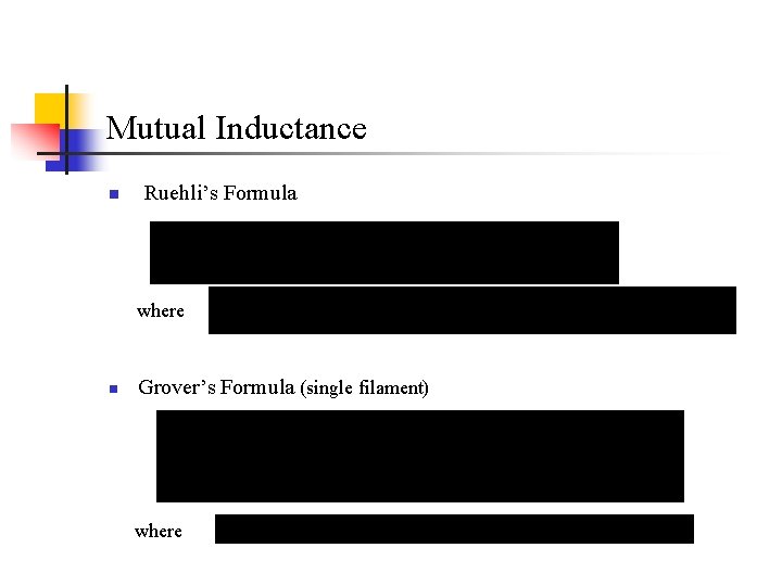
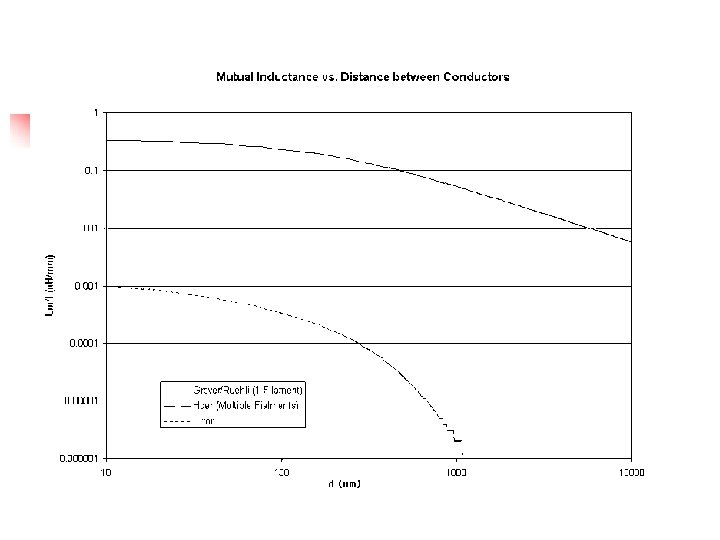
Mutual Inductance n Ruehli’s Formula where n Grover’s Formula (single filament) where
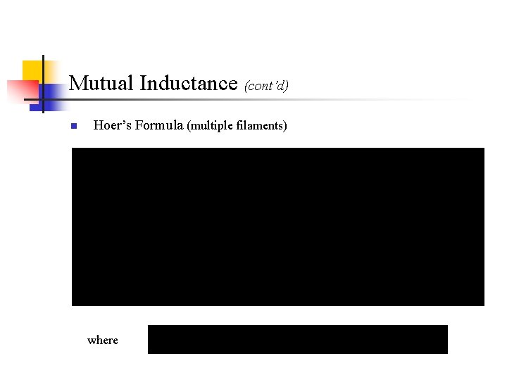
Mutual Inductance (cont’d) n Hoer’s Formula (multiple filaments) where
Conclusion n On-Chip inductance becomes a troublemaker in high-performance VLSI design ü n The concept of partial inductance is useful in VLSI area ü ü n Higher clock frequency, wide interconnections, complex return paths Not related to the return path Only dependent of geometry Several inductance formulae are in hand but they have ü ü Different computational complexities Different applicable ranges according to the geometry