Neel IRAM KIDs Array Cryostat Filters Cold electronics
- Slides: 22

Neel IRAM KIDs Array - Cryostat - Filters - Cold electronics - Measurement methods and assumptions for Sensitivity calculation - Antenna-coupled 42 pixels KIDs (first option) - 32 pixels LEKIDs (second option) - 196 pixels LEKIDs (TBT) - Best LEKIDs pixel tested in Cardiff (for 2010 …)

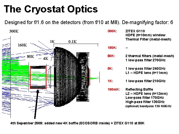
The Cryostat Optics Designed for f/1. 6 on the detectors (from f/10 at M 8). De-magnifying factor: 6 300 K 1 K 160 K 80 K 4 K 300 K: ZITEX G 110 HDPE (t=10 mm) window Thermal Filter (metal-mesh) 150 K: -- 80 K: 2 thermal filters (metal-mesh) 1 low-pass filter 270 GHz 5 K: 1 low-pass filter 240 GHz L 1 – HDPE lens (t=11 mm) 1 K: 1 low-pass filter 210 GHz 100 m. K: Reflecting Baffle L 2 – HDPE lens (t=12 mm) Low-pass filter 170 GHz High-pass filter 130 GHz 0. 1 K (optional) bandpass 130 -160 GHz optional) bandpass 4 th Sepember 2009: added new 4 K baffle (ECOSORB inside) + ZITEX G 110 at 80 K

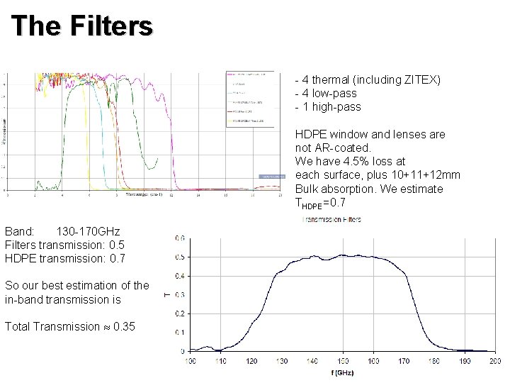
The Filters - 4 thermal (including ZITEX) - 4 low-pass - 1 high-pass HDPE window and lenses are not AR-coated. We have 4. 5% loss at each surface, plus 10+11+12 mm Bulk absorption. We estimate THDPE=0. 7 Band: 130 -170 GHz Filters transmission: 0. 5 HDPE transmission: 0. 7 So our best estimation of the in-band transmission is Total Transmission 0. 35

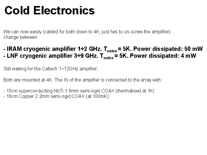
Cold Electronics We can now easily (cabled for both down to 4 K, just has to un-screw the amplifier) change between: - IRAM cryogenic amplifier 1÷ 2 GHz. Tnoise = 5 K. Power dissipated: 50 m. W - LNF cryogenic amplifier 3÷ 9 GHz. Tnoise = 5 K. Power dissipated: 4 m. W Still waiting for the Caltech 1÷ 12 GHz amplifier. Both are mounted at 4 K. The IN of the amplifier is connected to the array with: - 15 cm superconducting Nb. Ti 1. 6 mm semi-rigid COAX (thermalised at 1 K) - 16 cm Copper 2. 2 mm semi-rigid COAX (at 100 m. K)

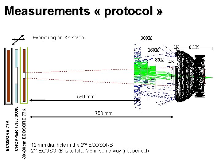
Measurements « protocol » Everything on XY stage 300 K 160 K 1 K 80 K 4 K 30 x 30 cm ECOSORB 77 K CHOPPER 77 K / 300 K ECOSORB 77 K 580 mm 750 mm 12 mm dia. hole in the 2 nd ECOSORB is to fake M 8 in some way (not perfect) 0. 1 K

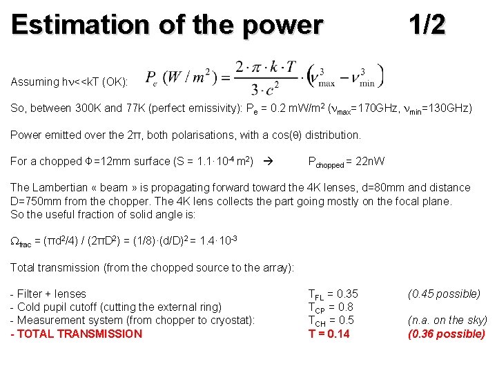
Estimation of the power 1/2 Assuming h <<k. T (OK): So, between 300 K and 77 K (perfect emissivity): Pe = 0. 2 m. W/m 2 ( max=170 GHz, min=130 GHz) Power emitted over the 2π, both polarisations, with a cos( ) distribution. For a chopped Φ=12 mm surface (S = 1. 1· 10 -4 m 2) Pchopped = 22 n. W The Lambertian « beam » is propagating forward toward the 4 K lenses, d=80 mm and distance D=750 mm from the chopper. The 4 K lens collects the part going mostly on the focal plane. So the useful fraction of solid angle is: frac = (πd 2/4) / (2πD 2) = (1/8)·(d/D)2 = 1. 4· 10 -3 Total transmission (from the chopped source to the array): - Filter + lenses - Cold pupil cutoff (cutting the external ring) - Measurement system (from chopper to cryostat): - TOTAL TRANSMISSION TFL = 0. 35 TCP = 0. 8 TCH = 0. 5 T = 0. 14 (0. 45 possible) (n. a. on the sky) (0. 36 possible)

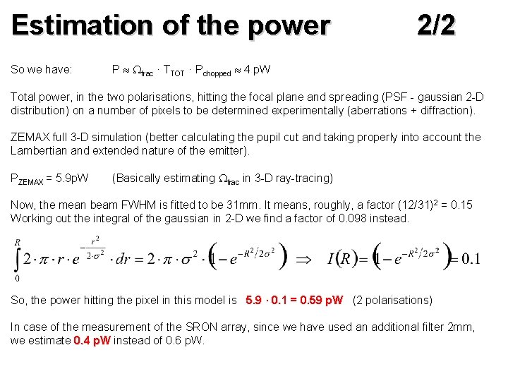
Estimation of the power So we have: 2/2 P frac · TTOT · Pchopped 4 p. W Total power, in the two polarisations, hitting the focal plane and spreading (PSF - gaussian 2 -D distribution) on a number of pixels to be determined experimentally (aberrations + diffraction). ZEMAX full 3 -D simulation (better calculating the pupil cut and taking properly into account the Lambertian and extended nature of the emitter). PZEMAX = 5. 9 p. W (Basically estimating frac in 3 -D ray-tracing) Now, the mean beam FWHM is fitted to be 31 mm. It means, roughly, a factor (12/31)2 = 0. 15 Working out the integral of the gaussian in 2 -D we find a factor of 0. 098 instead. So, the power hitting the pixel in this model is 5. 9 · 0. 1 = 0. 59 p. W (2 polarisations) p. W In case of the measurement of the SRON array, since we have used an additional filter 2 mm, we estimate 0. 4 p. W instead of 0. 6 p. W

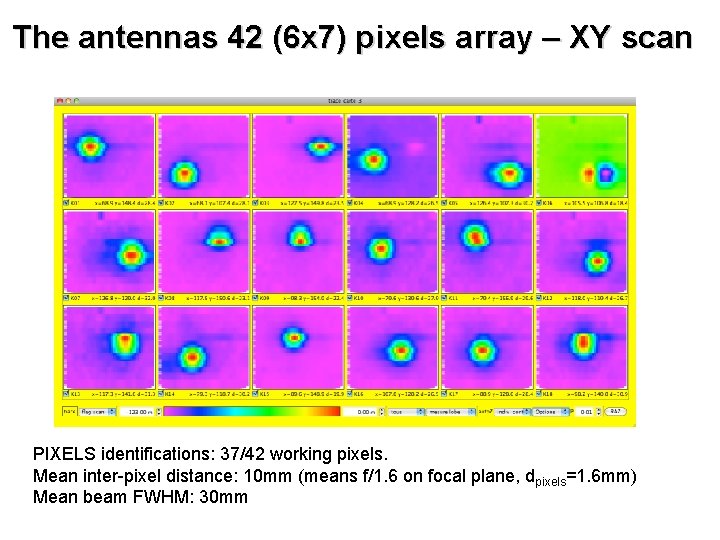
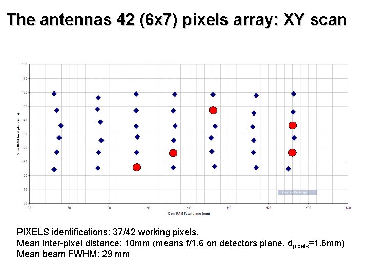
The antennas 42 (6 x 7) pixels array – XY scan PIXELS identifications: 37/42 working pixels. Mean inter-pixel distance: 10 mm (means f/1. 6 on focal plane, dpixels=1. 6 mm) Mean beam FWHM: 30 mm

The antennas 42 (6 x 7) pixels array: XY scan PIXELS identifications: 37/42 working pixels. Mean inter-pixel distance: 10 mm (means f/1. 6 on detectors plane, dpixels=1. 6 mm) Mean beam FWHM: 29 mm

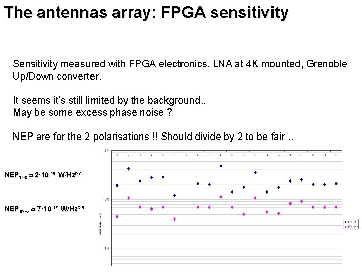
The antennas array: FPGA sensitivity Sensitivity measured with FPGA electronics, LNA at 4 K mounted, Grenoble Up/Down converter. It seems it’s still limited by the background. . May be some excess phase noise ? NEP are for the 2 polarisations !! Should divide by 2 to be fair. . NEP 1 Hz 2· 10 -15 W/Hz 0. 5 NEP 10 Hz 7· 10 -16 W/Hz 0. 5

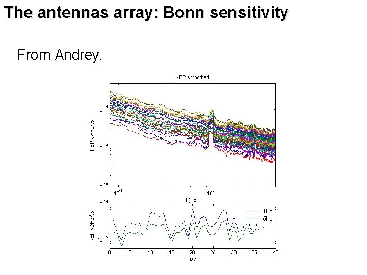
The antennas array: Bonn sensitivity From Andrey.

Antennas MKIDs next steps • Improve f-distribution (possible before Oct) – Change to optimum f-distribution on chip – Use e-beam mask (current is optical) • Improve coupling – – Current lens array E=2. 7 instead of 5 (loss 3 d. B) Change extension length (possible before Oct) Change lens material (Spring) Possible to Niquist reduce oversampling (max gain 6 d. B) • Improve F-noise – Integrate capacitor at coupler (demonstrated at JPL) improves phase noise by 10 d. B • Multi frequency pixels (+ kid parametric optimization) • Optimise for operation under sky loading

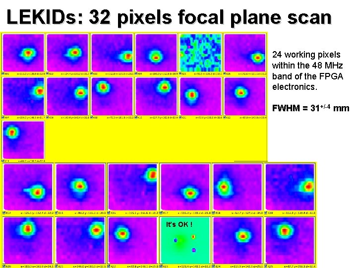
LEKIDs: 32 pixels focal plane scan 24 working pixels within the 48 MHz band of the FPGA electronics. FWHM = 31+/-4 mm It’s OK !

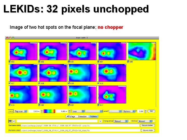
LEKIDs: 32 pixels unchopped Image of two hot spots on the focal plane; no chopper

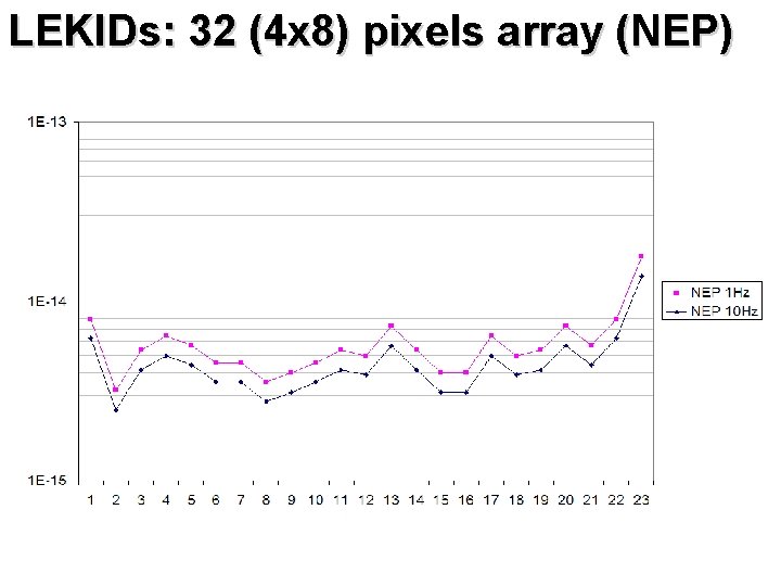
LEKIDs: 32 (4 x 8) pixels array (NEP)

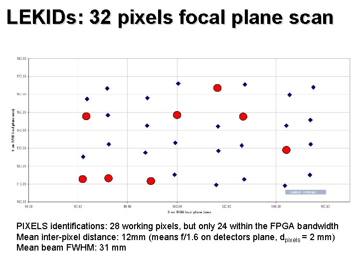
LEKIDs: 32 pixels focal plane scan PIXELS identifications: 28 working pixels, but only 24 within the FPGA bandwidth Mean inter-pixel distance: 12 mm (means f/1. 6 on detectors plane, dpixels = 2 mm) Mean beam FWHM: 31 mm

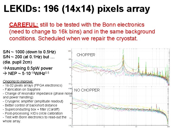
LEKIDs: 196 (14 x 14) pixels array CAREFUL: still to be tested with the Bonn electronics (need to change to 16 k bins) and in the same background conditions. Scheduled when we repair the cryostat. S/N ~ 1000 (down to 0. 5 Hz) S/N ~ 200 (at 0. 1 Hz) but … (dia. pupil 2 cm) Assuming 0. 5 p. W power NEP ~ 5· 10 -16 W/Hz 0. 5 CHOPPER Ongoing to improve: - 16 -32 pixels arrays (FPGA electronics) - Fabrication on Sapphire NO CHOPPER - Change of resonator impedance (phase noise and power handling) - Cryogenic amplifier (amplitude readout) - Better control of backshort distance - Superconducting box + filter (Cardiff) - Post-processing: KIDs circle calibration - Test with Bonn electronics to read-out the whole array.

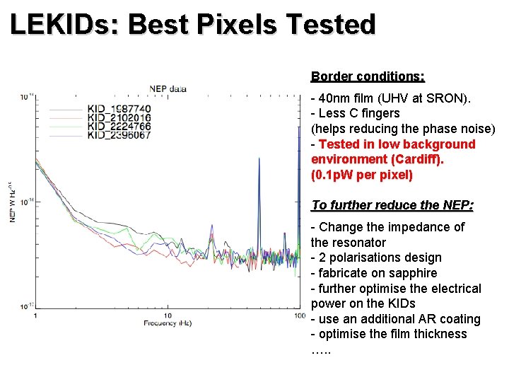
LEKIDs: Best Pixels Tested Border conditions: - 40 nm film (UHV at SRON). - Less C fingers (helps reducing the phase noise) - Tested in low background environment (Cardiff). (0. 1 p. W per pixel) To further reduce the NEP: - Change the impedance of the resonator - 2 polarisations design - fabricate on sapphire - further optimise the electrical power on the KIDs - use an additional AR coating - optimise the film thickness …. .

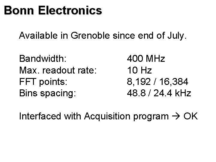
Bonn Electronics Available in Grenoble since end of July. Bandwidth: Max. readout rate: FFT points: Bins spacing: 400 MHz 10 Hz 8, 192 / 16, 384 48. 8 / 24. 4 k. Hz Interfaced with Acquisition program OK

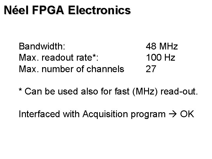
Néel FPGA Electronics Bandwidth: Max. readout rate*: Max. number of channels 48 MHz 100 Hz 27 * Can be used also for fast (MHz) read-out. Interfaced with Acquisition program OK

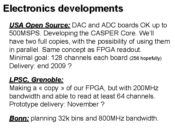
Electronics developments USA Open Source: DAC and ADC boards OK up to Source: 500 MSPS. Developing the CASPER Core. We’ll have two full copies, with the possibility of using them in parallel. Same concept as FPGA readout. Minimal goal: 128 channels each board (256 hopefully) Delivery: end 2009 ? LPSC, Grenoble: Making a « copy » of our FPGA, but with 200 MHz bandwidth and able to read at least 64 channels. Prototype delivery: November ? Bonn: planning 32 k bins and 800 MHz bandwidth. Bonn:

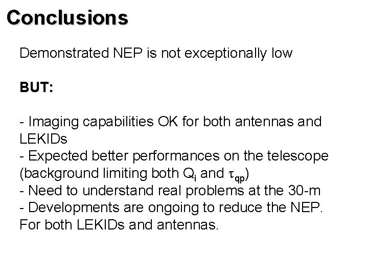
Conclusions Demonstrated NEP is not exceptionally low BUT: - Imaging capabilities OK for both antennas and LEKIDs - Expected better performances on the telescope (background limiting both Qi and qp) - Need to understand real problems at the 30 -m - Developments are ongoing to reduce the NEP. For both LEKIDs and antennas.