NANO MATERIALS Mr Sonaji V Gyakwad Assistant Professor

- Slides: 16

NANO MATERIALS Mr. Sonaji V. Gyakwad Assistant Professor Dept of Chemistry Mrs. K. S. K College Beed

Presentation Contents �Introduction � Methods of synthesis � 1. High energy ball milling � 2. Physical Vapor deposition (PVD) � 3. Physical Vapor deposition (CVD) � 4. Micro-emulsion � 5. Synthesis using micro-organisam and plant extract

Introduction �The word nano is a Greek word for dwarf. It indicates Billionth of some thing. �A Nanometer is a billionth of meter. �It is 100000 th the diameter of human hair. �Nanotechnology refers to the technology of rearranging and processing of atoms and molecules to fabricate materials to nanospecificasion such as nanomaterials.

�The range of nanotechnology lies between 1 to 100 nanometers. �The diameter of one hydrogen atom is 0. 1 nm. �The width of DNA Molecule is 2. 5 nm. � Glucose is just below 1 nm in size. �Several polymers upto 100 nm. �It is known that all things are made from atom. �The properties of materials are depends on how their atoms are arranged at the nano scale. �If any one of an atoms are rearranaged than a new objects is from.

�There has been explosive growth of nanoscience and technologyin the last five years. Primarily because of availabilities of new strategies for the synthesis of nonmaterial's. �Nanotechnology is a interdisciplinary subjects it includes like chemistry, physics, biology, material science and engineering. �Impact of this technology would be global and will be visible in the nature of food, clothing, shelter, transport, communication, drugs, disease detection and prevention. �Nanotechnology to bring out entirely new generation products cleaner, stranger, lighter, and ecofriendly.

The two main areas of nanotechnology are: �The wet area: This area includes biological domain. Nanostructures may functions within biological cells. �The Dry area: This area consists of water repellant architectures that helps improvement of materials including computer chips. �This technology is helps to arrive powerful computers availability. �The next generation of super computers will have more than a million processors which ha scapable of billion of operations per seconds.

�The properties of matter is depends on its size. The nature of matter on nanoscale is dramatically different from its bulk form. Its optical, electrical and colour properties will be differents.

Classification of Nanostructures �The classification of nonmaterial's on the basis of number of dimensions which lie within the molecules. �They are classified into three classes One dimensional: In this class the atoms arranged in a molecules in one dimensional form. Ex. Grain boundary films. Semiconductor quantum wells and super lattices. � 1. � 2. Two Dimensional: In this class the atoms arranged in a molecules in two dimensional form Ex. carbon nanotubes and nanofilaments, metal and magnetic nanowires. � 3. Three Dimensional: In this class the atoms arranged in a molecules in Three dimensional form. For Ex. Fullerenes, activated carbon, colloidal particals.

Methods of synthesis �There are two ways for the synthesis of nanomaterials � 1. Top down method � 2. bottom up method �The top down approach milling of smaller structures from larger one is carried out. �The bottom up approach of fabricating materials was originally given by Richard Finman. �In his approach the fabrication materials and devices of the atomic and molecular scale by self organization. Transistors are made by this approach.

Top down /High energy ball milling �It is also known as mechanical alloying process �Grained metals, ceramics and polymers are taken in the form of powder and are crushed mechanically in rotating drums by hard steel or tungsten carbide balls under controlled atmospheric conditions. Which prevent unwanted oxidation during rotation.

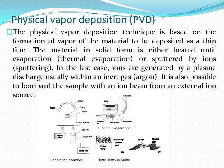
Physical vapor deposition (PVD) �The physical vapor deposition technique is based on the formation of vapor of the material to be deposited as a thin film. The material in solid form is either heated until evaporation (thermal evaporation) or sputtered by ions (sputtering). In the last case, ions are generated by a plasma discharge usually within an inert gas (argon). It is also possible to bombard the sample with an ion beam from an external ion source.

�Another PVD Process is direct gas phase condensation. The metal is taken in temperature controlled crucible. The metal is evaporated in an inert gas environment ultra high vacuum inert gas condensation. Than the metal vapors cool through collision with inert gas species become supersaturated than nucleates homogeneously. �The particle 1 size in the range of 1 -100 nm

Chemical Vapour Deposition (CVD) � In this process thermal decomposition of gas phase species at 500 -1000 (Degree Celsius) Temperature. � On the substrate placed inside a reactor a solid material condenses due to chemical reactions between source gases introduced into the reactor. � The two most important CVD technologies are the Low Pressure CVD (LPCVD) and Plasma Enhanced CVD (PECVD). � The PECVD process can operate at lower temperatures (down to 300° C) thanks to the extra energy supplied to the gas molecules by the plasma in the reactor. However, the quality of the films tend to be inferior to processes running at higher temperatures. The material is deposited on one side of the wafers.

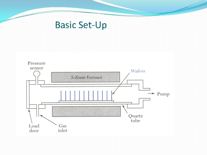
� The LPCVD process produces layers with excellent uniformity of thickness and material characteristics. � The main problems with the process are the high deposition temperature (higher than 600°C) and the relatively slow deposition rate. � The material is deposited on both sides of the substrates (wafers).

Basic Set-Up

Thanks for your attention