MAPS readout electronics for Vertex Detectors ILC A

- Slides: 21
MAPS read-out electronics for Vertex Detectors (ILC) A low power and low signal 4 bit 50 MS/s double sampling pipelined ADC M. DAHOUMANE M. Dahoumane @ TWEPP 07 1
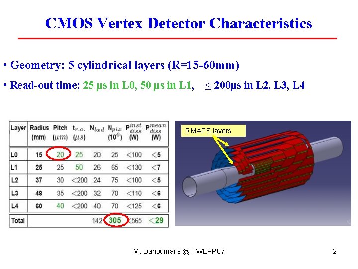
CMOS Vertex Detector Characteristics • Geometry: 5 cylindrical layers (R=15 -60 mm) • Read-out time: 25 µs in L 0, 50 µs in L 1, ≤ 200µs in L 2, L 3, L 4 5 MAPS layers M. Dahoumane @ TWEPP 07 2
MAPS array + read-out for ILC vertex detector Collaboration LPSC-IPHC ADC design requirements: • Small LSB 1 m. V • Narrow column wide 20 μm • Length <1 mm • Low power 0. 5 m. W • High speed >10 MHz/column M. Dahoumane @ TWEPP 07 3
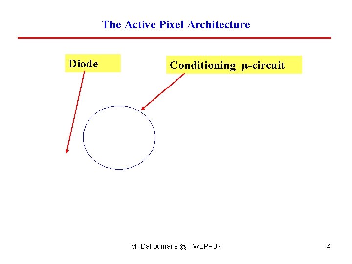
The Active Pixel Architecture Diode Conditioning µ-circuit M. Dahoumane @ TWEPP 07 4
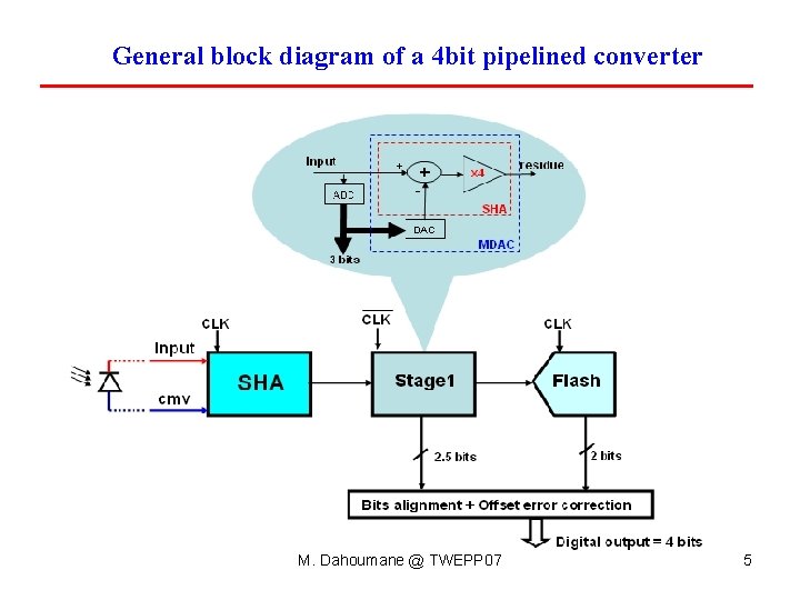
General block diagram of a 4 bit pipelined converter M. Dahoumane @ TWEPP 07 5
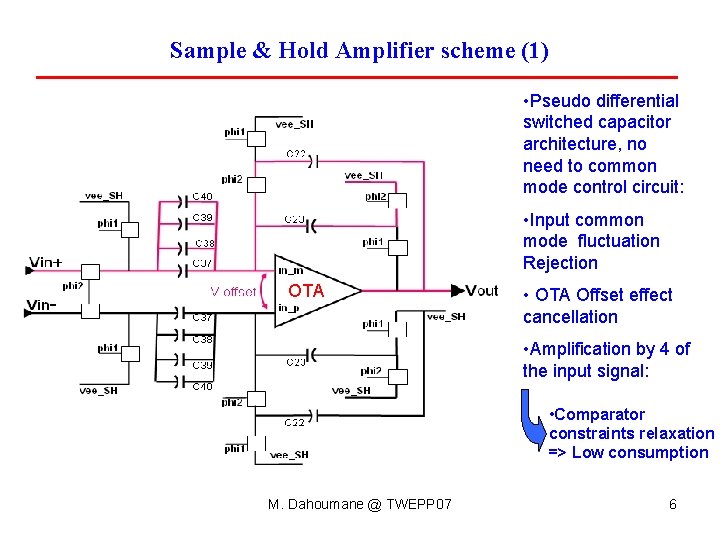
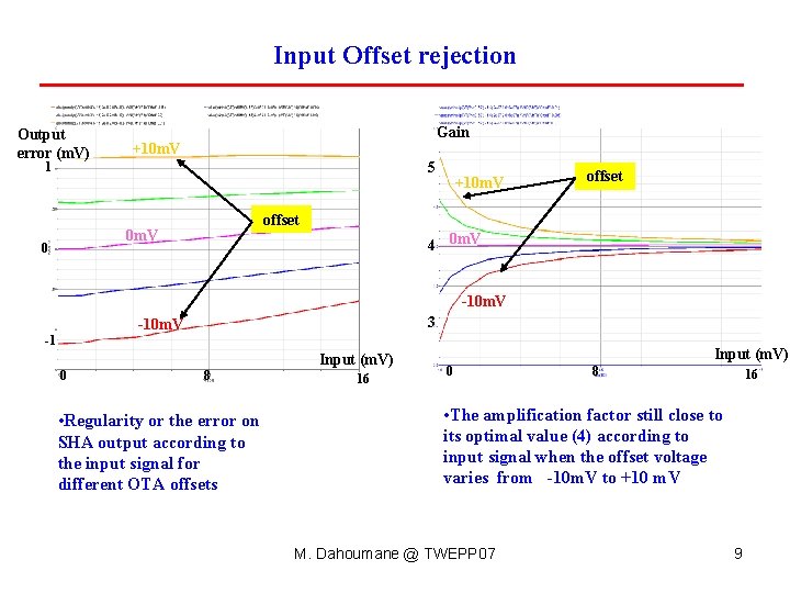
Sample & Hold Amplifier scheme (1) • Pseudo differential switched capacitor architecture, no need to common mode control circuit: • Input common mode fluctuation Rejection OTA • OTA Offset effect cancellation • Amplification by 4 of the input signal: • Comparator constraints relaxation => Low consumption M. Dahoumane @ TWEPP 07 6
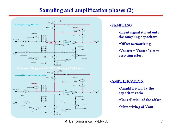
Sampling and amplification phases (2) • SAMPLING • Input signal stored onto the sampling capacitors • Offset memorizing • Vout(t) = Vout(t-1), non resetting effect • AMPLIFICATION • Amplification by the capacitor ratio • Cancellation of the offset • Memorizing of Vout M. Dahoumane @ TWEPP 07 7
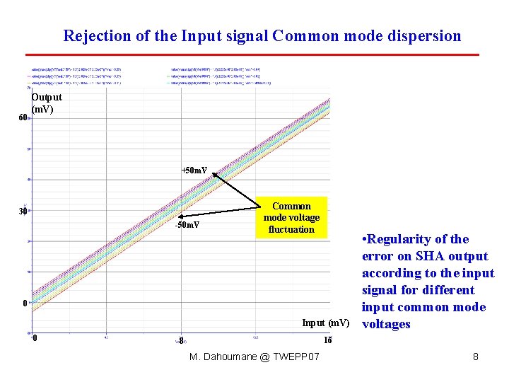
Rejection of the Input signal Common mode dispersion 60 Output (m. V) +50 m. V 30 -50 m. V Common mode voltage fluctuation 0 Input (m. V) 0 • Regularity of the error on SHA output according to the input signal for different input common mode voltages 16 8 M. Dahoumane @ TWEPP 07 8
Input Offset rejection Output error (m. V) Gain +10 m. V 5 1 offset 0 m. V 0 +10 m. V 4 0 m. V -10 m. V 3 -10 m. V -1 0 8 • Regularity or the error on SHA output according to the input signal for different OTA offsets Input (m. V) 16 Input (m. V) 0 8 16 • The amplification factor still close to its optimal value (4) according to input signal when the offset voltage varies from -10 m. V to +10 m. V M. Dahoumane @ TWEPP 07 9
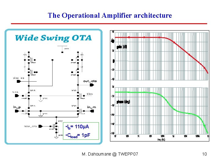
The Operational Amplifier architecture • Ib= 110µA • Cload= 1 p. F M. Dahoumane @ TWEPP 07 10
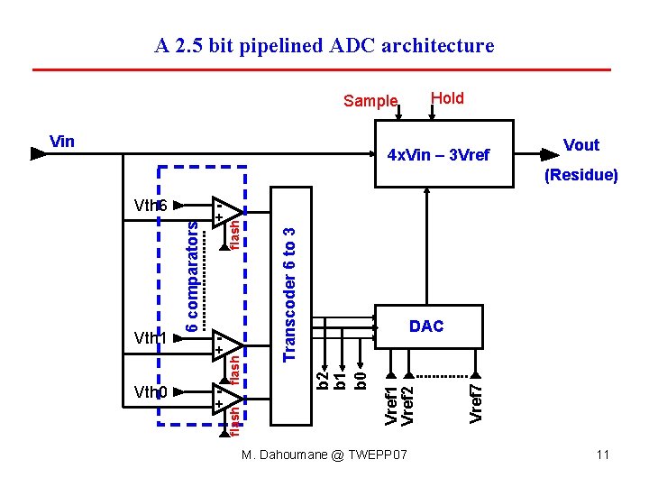
A 2. 5 bit pipelined ADC architecture Hold Sample Vin 4 x. Vin – 3 Vref Vout (Residue) Transcoder 6 to 3 M. Dahoumane @ TWEPP 07 Vref 1 Vref 2 DAC b 2 b 1 b 0 - + flash Vth 0 6 comparators Vth 1 + flash - Vth 6 11
High speed comparator scheme • composed of Three stages • Preamplifier: gain 10 • folded cascode stage • and flash stage • Low offset ( mc simulations: worse case ± 5 m. V) M. Dahoumane @ TWEPP 07 12
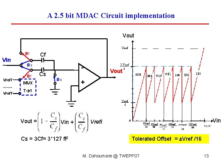
A 2. 5 bit MDAC Circuit implementation Vout øf Vin Vref 7 ……. . Vref 1 Cf øs øf MUX Cs øs Vout + 7 1 Vout = Vin + Cs = 3 Cf= 3*127 f. F Vin Vrefi Tolerated Offset = ±Vref /16 M. Dahoumane @ TWEPP 07 13
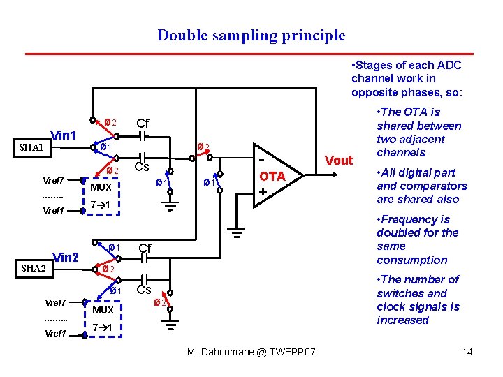
Double sampling principle • Stages of each ADC channel work in opposite phases, so: Vin 1 SHA 1 Vref 7 ……. . Vref 1 SHA 2 Vin 2 ø 1 ø 2 ……. . . Vref 1 ø 2 Cs ø 1 MUX 7 1 ø 1 OTA + Cf MUX Cs Vout • All digital part and comparators are shared also • Frequency is doubled for the same consumption ø 2 ø 1 Vref 7 Cf • The OTA is shared between two adjacent channels • The number of switches and clock signals is increased ø 2 7 1 M. Dahoumane @ TWEPP 07 14
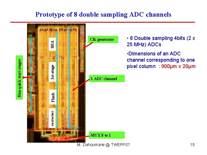
• 8 Double sampling 4 bits (2 x 25 MHz) ADCs • Dimensions of an ADC channel corresponding to one pixel column : 900µm x 20µm 1 ADC channel Flash 1 st stage Clk generator corrector Bias quick start stages SHA Prototype of 8 double sampling ADC channels MUX 8 to 1 M. Dahoumane @ TWEPP 07 15
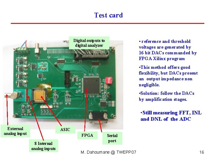
Test card Digital outputs to digital analyzer • reference and threshold voltages are generated by 16 bit DACs commanded by FPGA Xilinx program • This method offers good flexibility, but DACs present an output impedance non negligible. • Solution: follow the DACs by amplification stages. • Still measuring FFT, INL and DNL of the ADC External analog input ASIC FPGA 8 Internal analog inputs Serial port M. Dahoumane @ TWEPP 07 16
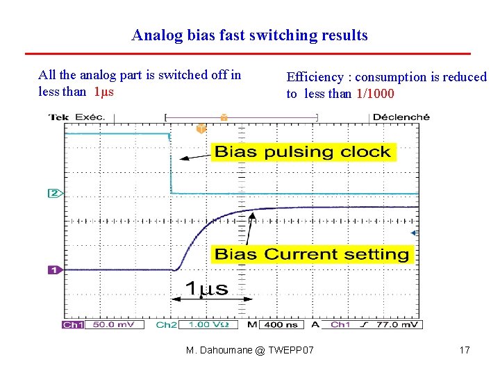
Analog bias fast switching results All the analog part is switched off in less than 1µs Efficiency : consumption is reduced to less than 1/1000 M. Dahoumane @ TWEPP 07 17
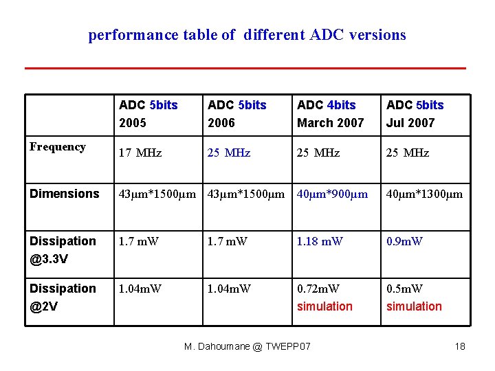
performance table of different ADC versions Frequency ADC 5 bits 2005 ADC 5 bits 2006 ADC 4 bits March 2007 ADC 5 bits Jul 2007 17 MHz 25 MHz Dimensions 43µm*1500µm 40µm*900µm 40µm*1300µm Dissipation @3. 3 V 1. 7 m. W 1. 18 m. W 0. 9 m. W Dissipation @2 V 1. 04 m. W 0. 72 m. W simulation 0. 5 m. W simulation M. Dahoumane @ TWEPP 07 18
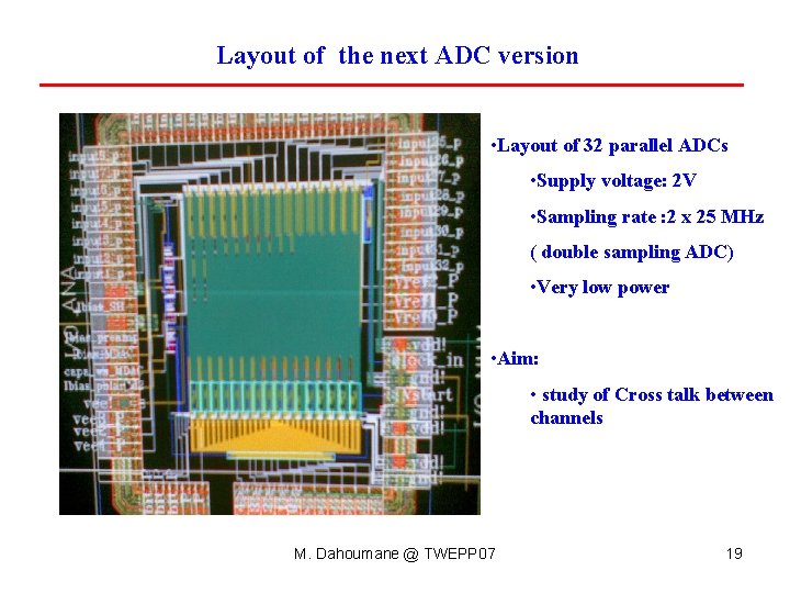
Layout of the next ADC version • Layout of 32 parallel ADCs • Supply voltage: 2 V • Sampling rate : 2 x 25 MHz ( double sampling ADC) • Very low power • Aim: • study of Cross talk between channels M. Dahoumane @ TWEPP 07 19
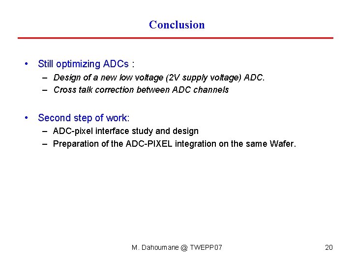
Conclusion • Still optimizing ADCs : – Design of a new low voltage (2 V supply voltage) ADC. – Cross talk correction between ADC channels • Second step of work: – ADC-pixel interface study and design – Preparation of the ADC-PIXEL integration on the same Wafer. M. Dahoumane @ TWEPP 07 20
THANK YOU FOR YOUR ATTENTION! M. Dahoumane @ TWEPP 07 21