Length Scale of Imperfections Line Defects Dislocations and
- Slides: 25

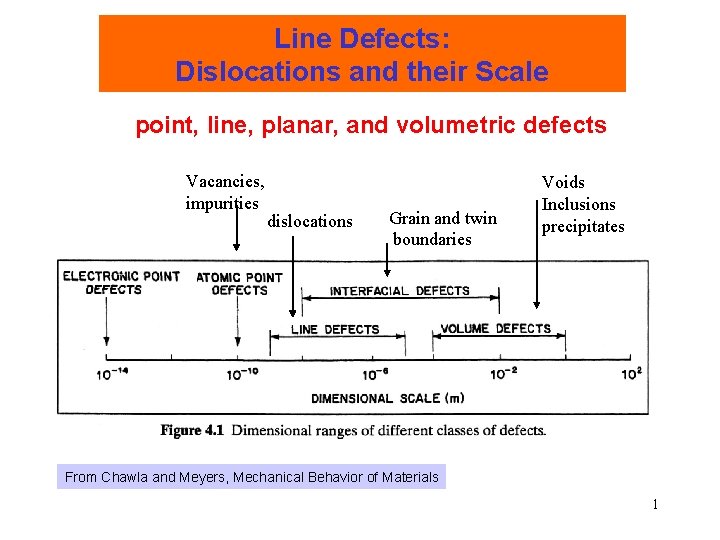
Length Scale of Imperfections Line Defects: Dislocations and their Scale point, line, planar, and volumetric defects Vacancies, impurities dislocations Grain and twin boundaries Voids Inclusions precipitates From Chawla and Meyers, Mechanical Behavior of Materials 1

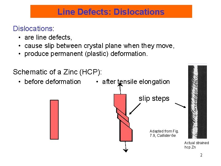
Line Defects: Dislocations: • are line defects, • cause slip between crystal plane when they move, • produce permanent (plastic) deformation. Schematic of a Zinc (HCP): • before deformation • after tensile elongation slip steps Adapted from Fig. 7. 9, Callister 6 e. Actual strained hcp Zn 2

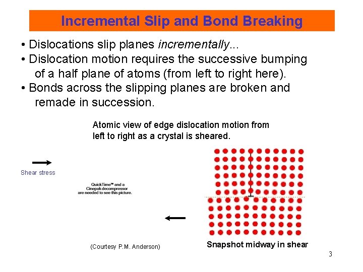
Incremental Slip and Bond Breaking • Dislocations slip planes incrementally. . . • Dislocation motion requires the successive bumping of a half plane of atoms (from left to right here). • Bonds across the slipping planes are broken and remade in succession. Atomic view of edge dislocation motion from left to right as a crystal is sheared. Shear stress (Courtesy P. M. Anderson) Snapshot midway in shear 3

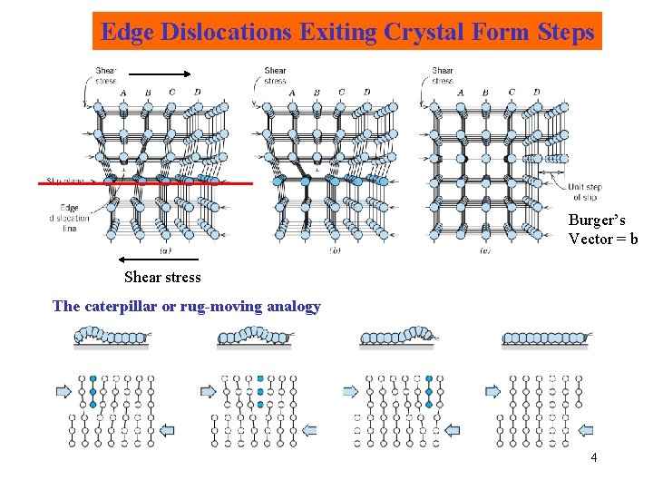
Edge Dislocations Exiting Crystal Form Steps Burger’s Vector = b Shear stress The caterpillar or rug-moving analogy 4

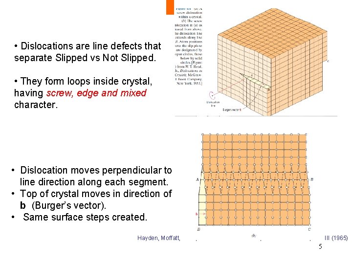
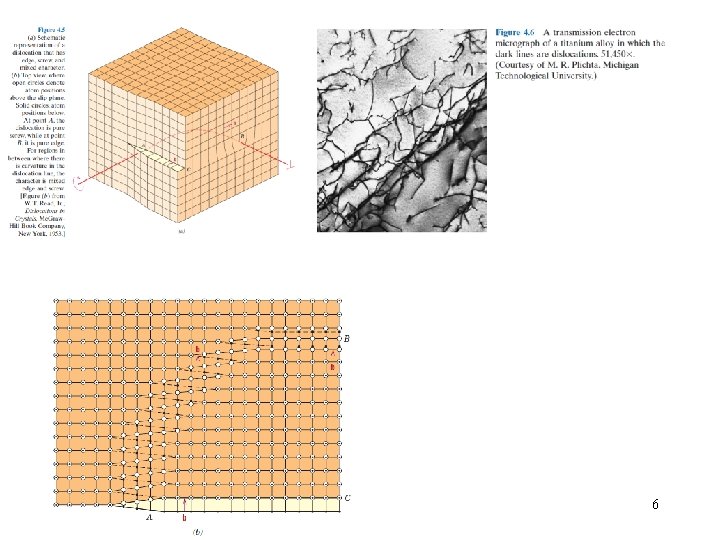
• Dislocations are line defects that separate Slipped vs Not Slipped. • They form loops inside crystal, having screw, edge and mixed character. • Dislocation moves perpendicular to line direction along each segment. • Top of crystal moves in direction of b (Burger’s vector). • Same surface steps created. Hayden, Moffatt, Wulff, “The Structure and Properties of Materials, ” Vol III (1965) 5

6

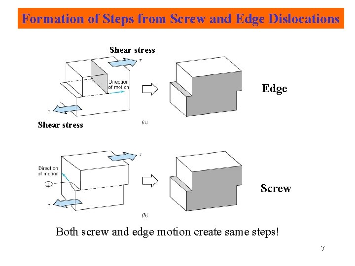
Formation of Steps from Screw and Edge Dislocations Shear stress Edge Shear stress Screw Both screw and edge motion create same steps! 7

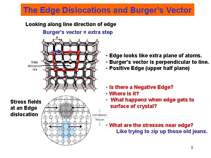
The Edge Dislocations and Burger’s Vector Looking along line direction of edge Burger’s vector = extra step • Edge looks like extra plane of atoms. • Burger’s vector is perpendicular to line. • Positive Edge (upper half plane) Stress fields at an Edge dislocation • Is there a Negative Edge? • Where is it? • What happens when edge gets to surface of crystal? • What are the stresses near edge? Like trying to zip up those old jeans. 8

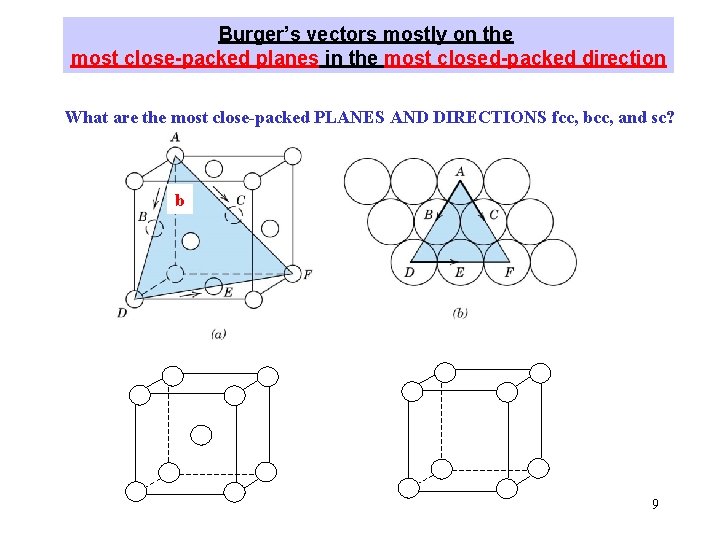
Burger’s vectors mostly on the most close-packed planes in the most closed-packed direction What are the most close-packed PLANES AND DIRECTIONS fcc, bcc, and sc? b 9

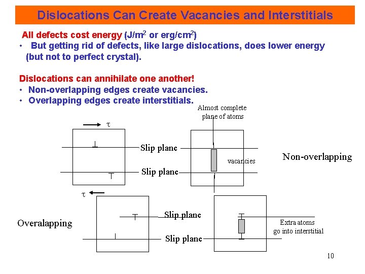
Dislocations Can Create Vacancies and Interstitials All defects cost energy (J/m 2 or erg/cm 2) • But getting rid of defects, like large dislocations, does lower energy (but not to perfect crystal). Dislocations can annihilate one another! • Non-overlapping edges create vacancies. • Overlapping edges create interstitials. Almost complete plane of atoms Slip plane vacancies Slip plane Non-overlapping Overalapping Slip plane Extra atoms go interstitial 10

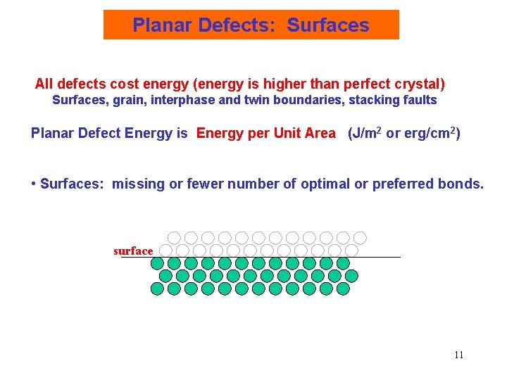
Planar Defects: Surfaces All defects cost energy (energy is higher than perfect crystal) Surfaces, grain, interphase and twin boundaries, stacking faults Planar Defect Energy is Energy per Unit Area (J/m 2 or erg/cm 2) • Surfaces: missing or fewer number of optimal or preferred bonds. surface 11

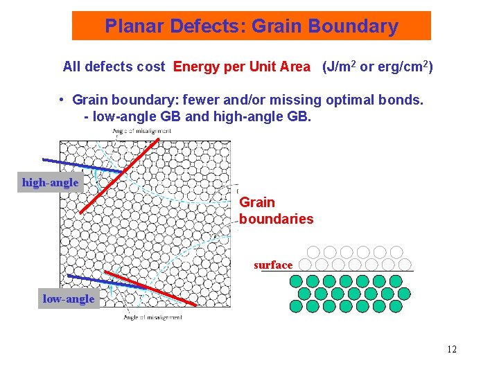
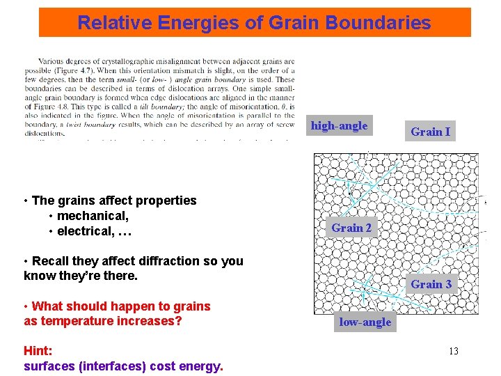
Planar Defects: Grain Boundary All defects cost Energy per Unit Area (J/m 2 or erg/cm 2) • Grain boundary: fewer and/or missing optimal bonds. - low-angle GB and high-angle GB. high-angle Grain boundaries surface low-angle 12

Relative Energies of Grain Boundaries high-angle • The grains affect properties • mechanical, • electrical, … Grain 2 • Recall they affect diffraction so you know they’re there. • What should happen to grains as temperature increases? Hint: surfaces (interfaces) cost energy. Grain I Grain 3 low-angle 13

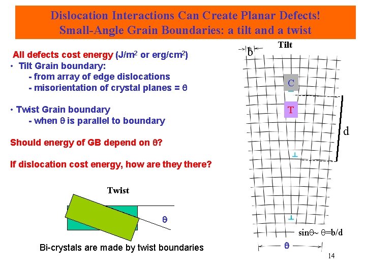
Dislocation Interactions Can Create Planar Defects! Small-Angle Grain Boundaries: a tilt and a twist All defects cost energy (J/m 2 or erg/cm 2) • Tilt Grain boundary: - from array of edge dislocations - misorientation of crystal planes = • Twist Grain boundary - when is parallel to boundary b Tilt C T d Should energy of GB depend on ? If dislocation cost energy, how are they there? Twist sin ~ =b/d Bi-crystals are made by twist boundaries 14

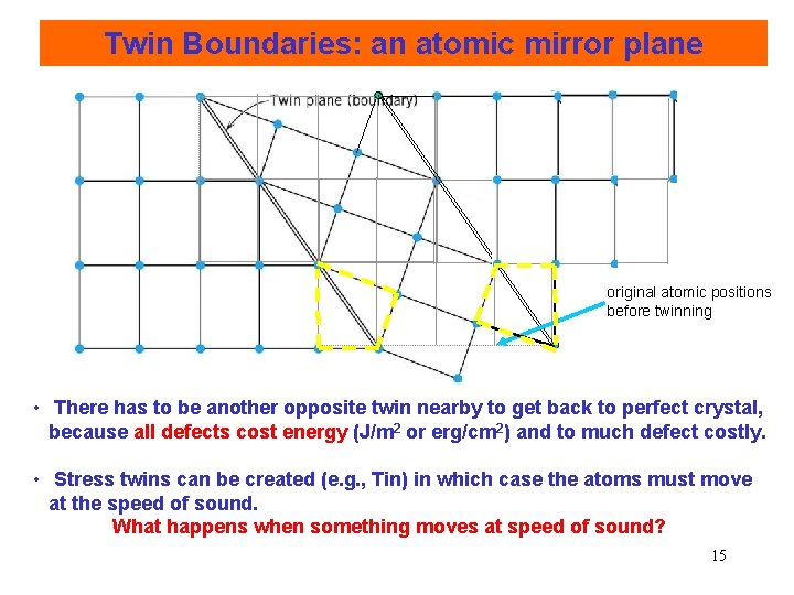
Twin Boundaries: an atomic mirror plane original atomic positions before twinning • There has to be another opposite twin nearby to get back to perfect crystal, because all defects cost energy (J/m 2 or erg/cm 2) and to much defect costly. • Stress twins can be created (e. g. , Tin) in which case the atoms must move at the speed of sound. What happens when something moves at speed of sound? 15

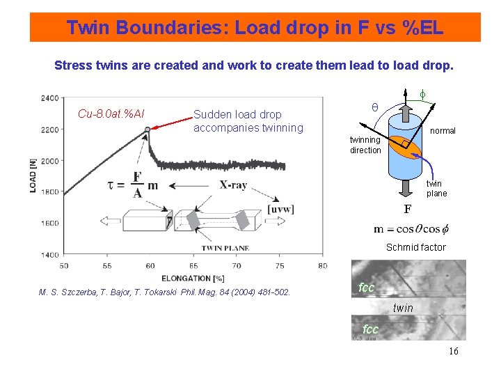
Twin Boundaries: Load drop in F vs %EL Stress twins are created and work to create them lead to load drop. Cu-8. 0 at. %Al Sudden load drop accompanies twinning f normal twinning direction twin plane F Schmid factor M. S. Szczerba, T. Bajor, T. Tokarski Phil. Mag. 84 (2004) 481 -502. fcc twin fcc 16

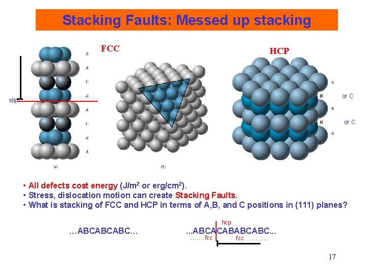
Stacking Faults: Messed up stacking FCC HCP or C slip or C • All defects cost energy (J/m 2 or erg/cm 2). • Stress, dislocation motion can create Stacking Faults. • What is stacking of FCC and HCP in terms of A, B, and C positions in (111) planes? hcp …ABCABCABC… . . . ABCACABABCABC. . . ……. fcc ………. . 17

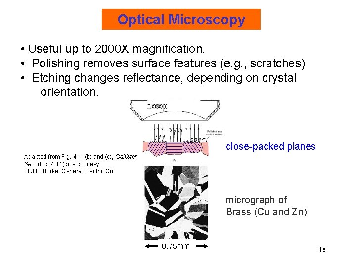
Optical Microscopy • Useful up to 2000 X magnification. • Polishing removes surface features (e. g. , scratches) • Etching changes reflectance, depending on crystal orientation. close-packed planes Adapted from Fig. 4. 11(b) and (c), Callister 6 e. (Fig. 4. 11(c) is courtesy of J. E. Burke, General Electric Co. micrograph of Brass (Cu and Zn) 0. 75 mm 18

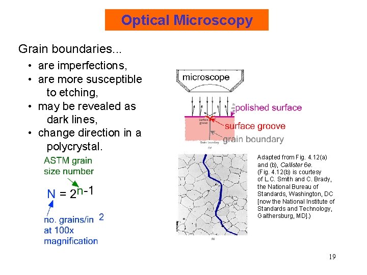
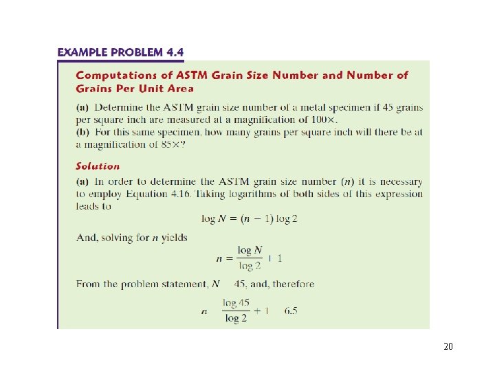
Optical Microscopy Grain boundaries. . . • are imperfections, • are more susceptible to etching, • may be revealed as dark lines, • change direction in a polycrystal. Adapted from Fig. 4. 12(a) and (b), Callister 6 e. (Fig. 4. 12(b) is courtesy of L. C. Smith and C. Brady, the National Bureau of Standards, Washington, DC [now the National Institute of Standards and Technology, Gaithersburg, MD]. ) 19

20

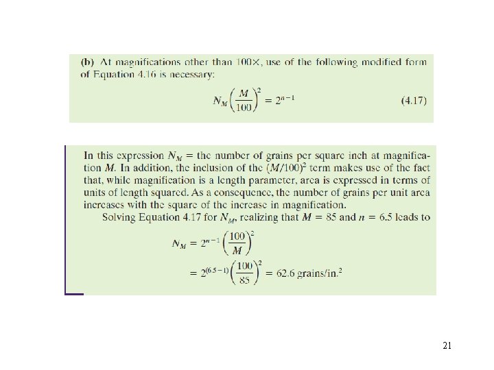
21

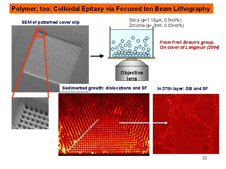
Polymer, too: Colloidal Epitaxy via Focused Ion Beam Lithography SEM of patterned cover slip Silica (f=1. 18 mm, 0. 5 vol%) Zirconia (f~ 3 nm, 0. 03 vol%) From Prof. Braun’s group. On cover of Langmuir (2004) Objective lens Sedimented growth: dislocations and SF In 37 th layer: GB and SF 22

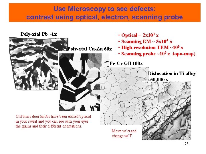
Use Microscopy to see defects: contrast using optical, electron, scanning probe Poly-xtal Pb ~1 x Poly-xtal Cu-Zn 60 x • Optical ~ 2 x 10³ x • Scanning EM ~ 5 x 10⁴ x • High-resolution TEM ~106 x • Scanning probe ~109 x topo-map) Fe-Cr GB 100 x Dislocation in Ti alloy ~50, 000 x Old brass door knobs have been etched by acid in your sweat and you can see with your eyes the grains and their different orientations. Move w/ and change w/ T 23

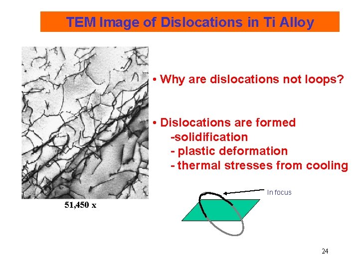
TEM Image of Dislocations in Ti Alloy • Why are dislocations not loops? • Dislocations are formed -solidification - plastic deformation - thermal stresses from cooling In focus 51, 450 x 24

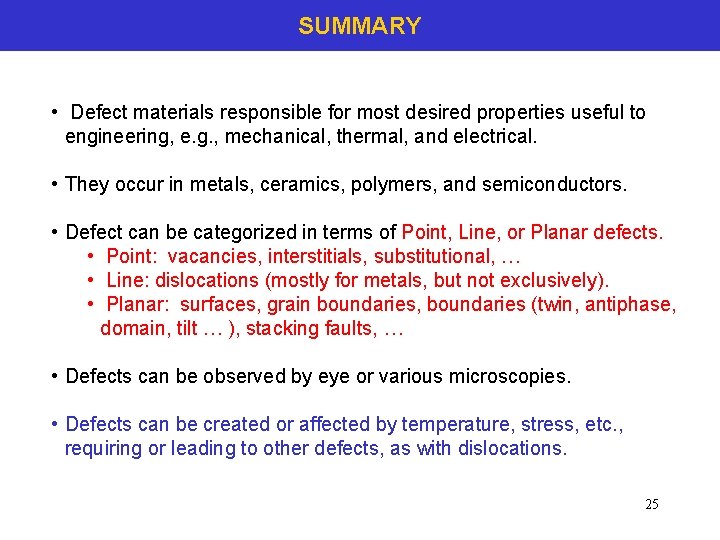
SUMMARY • Defect materials responsible for most desired properties useful to engineering, e. g. , mechanical, thermal, and electrical. • They occur in metals, ceramics, polymers, and semiconductors. • Defect can be categorized in terms of Point, Line, or Planar defects. • Point: vacancies, interstitials, substitutional, … • Line: dislocations (mostly for metals, but not exclusively). • Planar: surfaces, grain boundaries, boundaries (twin, antiphase, domain, tilt … ), stacking faults, … • Defects can be observed by eye or various microscopies. • Defects can be created or affected by temperature, stress, etc. , requiring or leading to other defects, as with dislocations. 25