JEDEC Standards Nicole Okamoto and Widah Saied All


.")
- Slides: 29
JEDEC Standards -Nicole Okamoto and Widah Saied All figures from Jedec Standard JESD 51 -12 www. jedec. org
JEDEC Introduction n JEDEC was founded in 1960 and stands for the Joint Electron Device Engineering Council. JEDEC is the standardization body of the Electronic Industries Alliance, which helps develop standards on electronic components, consumer electronics, electronic information, telecommunications, and internet security. JEDEC issues often used standards for device interfaces, such as RAM and DDR SDRAM(double-data-rate synchronous dynamic random access memory), which is a type of memory in integrated circuits used in computers. Wikipedia, http: //en. wikipedia. org/wiki/JEDEC
JEDEC Introduction n n JEDEC Philosophy: JEDEC standards and publications are designed to serve the public interest through eliminating misunderstandings between manufacturers and purchasers, facilitating interchangeability and improvement of products. JEDEC has 2700 participants, appointed by 270 companies work in 50 committees. The world community accepts the publications and standards that they generate. Jedec, http: //www. jedec. org/
Examples of standards n n n JESD 22 -A 103 C HIGH TEMPERATURE STORAGE LIFE: The test is applicable for evaluation, screening, monitoring, and/or qualification of all solid state devices. High Temperature storage test is typically used to determine the effect of time and temperature, under storage conditions, for thermally activated failure mechanisms of solid state electronic devices During the test elevated temperatures (accelerated test conditions) are used without electrical stress applied.
Examples of standards n n JESD 22 -A 104 C TEMPERATURE CYCLING: This standard provides a method for determining solid state devices capability to withstand extreme temperature cycling. JESD 22 -A 106 B THERMAL SHOCK: This test is conducted to determine the resistance of a part to sudden exposure to extreme changes in temperature and to the effect of alternate exposures to these extremes.
JESD 51 Methodology for the Thermal Measurement of Component Packages n n n n JESD 51 -1 Integrated Circuit Thermal Measurement Method – Electrical Test Method JESD 51 -2 Integrated Circuit Thermal Test Method Environmental Conditions – Natural Convection JESD 51 -3 Low Effective Thermal Conductivity Test Board for Leaded Surface Mount Packages JESD 51 -4 Thermal Test Chip Guideline JESD 51 -5 Extension of Thermal Test Board Standards for Packages with Direct Thermal Attachment Mechanisms JESD 51 -6 Integrated Circuit Thermal Test Method Environmental Conditions – Forced Convection JESD 51 -7 High Effective Thermal Conductivity Test Board for Leaded Surface Mount Packages
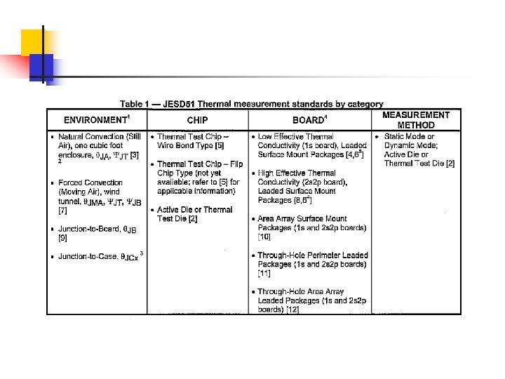
JESD 51 cont. n n n JESD 51 -8 Integrated Circuit Thermal Test Method Environmental Conditions – Junction to Board JESD 51 -9 Test Boards for Area Array Surface Mount Package Thermal Measurements JESD 51 -10 Test Boards for Through-Hole Perimeter Leaded Package Thermal Measurements JESD 51 -11 Test Boards for Through-Hole Area Array Leaded Package Thermal Measurements JESD 51 -12 Guidelines for Reporting and Using Electronic Package Thermal Information
JESD 22 -A 103 C High Temperature Storage Life n Scope: Determine the effect of time and temperature, under storage conditions, of thermally activated failure mechanisms of solid state electronic devices. Jedec Standard, http: //www. jedec. org/download/search/22 a 103 c. pdf
Apparatus of Test n The apparatus is a temperature controlled chamber capable of maintaining the entire sample population at a specified testing temperature.
Method of Testing n The samples will be stored at one of the temperature conditions given in Table 1: High Temperature Storage Conditions Condition A: +125(-0/+10) ºC Condition B: +150(-0/+10) ºC Condition C: +175(-0/+10) ºC Condition D: +200(-0/+10) ºC Condition E: +250(-0/+10) ºC Condition F: +300(-0/+10) ºC Condition G: +85(-0/+10) ºC
Method of Testing n n n Typically, the sample is tested under condition B for 1000 hours, but other conditions or durations may be used. Note: the rate of temperature increase should be low to prevent overstress of the sample that would not occur under normal conditions. The failure criteria for a sample is: n n The part can no longer function as designed Cracking, chipping, or breaking of the package as long as the package performance was critical to the performance of the sample. However, if the damage was due to fixtures or handling, then failure is not attributed to the test.
Method of Testing n Things to be specified: n n n Sample size and number of failures Time and conditions Whether intermediate measurements were taken
JESD 51 -12 Guidelines for Reporting and Using Electronic Package Thermal Information n q. JA junction-to-still ambient air resistance (natural convection n q. JMA junction-to-moving air resistance (forced convection)
Deviations During Application n Results during application may vary since the application may differ from the following test conditions: n n n n Power dissipation Air velocity, direction, turbulence Power and number of adjacent components and boards PCB orientation and size Two-sided vs. one-sided mounting Die size Copper trace thickness and widths Environment (for example, natural convection tests are done in a chamber 1 ft 3)
Conduction resistances n n qjctop, qjcbot – junction to top of case and bottom of case resistances, respectively qjb – junction to board resistances n n n Leaded package: measure Tboard to foot of lead Surface mount package: measure board trace within 1 mm of package These resistances are found by forcing all of the heat flow to go out the respective surface, which may not match reality
Thermal Characterization Parameter n n ΨJT – junction to top thermal characterization ΨJB – junction to board thermal characterization The equations are the same as those for thermal resistance q except that the power P is now the total power, not just the power in that direction. For example, if only 5% of your total heat loss is down through the PCB, your P would still be your total power. These can help with estimates of junction temperature for object already under use where temperatures can be measured and there is no heat sink present (instead of for the design phase)
Compact Models n Two-resistor model: good for hand calculations but not really accurate
DELPHI Compact Models n n These are mathematical models, not thermal resistance model Provided by some component manufacturers
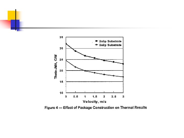
Effect of Package Construction on Thermal Results n n 2 s 0 p: two signal planes, zero power planes on laminate substrate for plastic ball grid array packages Added copper improves performance
Effect of PCB Design n More copper to spread heat means better performance.
Effect of Multiple Packages
Effect of PCB size n On setups where a lot of heat is carried away by the copper in the PCB, the larger the PCB the better the performance – more heat transfer area.
Effect of Die Size n n For the same power, larger dies have a smaller heat flux and hence better performance. Smaller dies tend to be cheaper, though. a) PBGA package (plastic) b) ceramic flip chip
Effect of Die Power Level n As power levels go up, so do surface temperatures. This increases natural convection and radiation, decreasing q. JA
Reporting Requirement Examples
Reporting Requirement Examples
Reference n n Jedec the Standards Resource for the World Semiconductor Industry (October 2006). http: //www. jedec. org. Jedec Standard JESD 22 -A 103 C High Temperature Storage Temperature. Retrieved October 2006. http: //www. jedec. org/download/search/22 a 103 c. pdf. Jedec Standard JESD 51 -12 Guidelines for Reporting and Using Electronic Package Thermal Information. Retreived October 2006. www. jedec. org. Wikipedia the Free Encyclopedia(October 2006). Jedec. Retrieved October 2006. http: //en. wikipedia. org/wiki/JEDEC.