Graphene Rachel Wooten Department of Physics Solid State
- Slides: 17

Graphene Rachel Wooten Department of Physics Solid State Physics II March 6, 2008 Taught by Professor Dagotto rwooten 1@utk. edu

Outline • What is graphene? • How it is made • Properties – Electronic & physical properties – Relativistic charge carriers – Anomalous quantum Hall effect • Future Applications

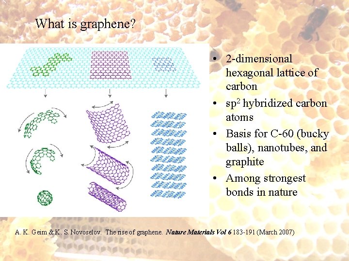
What is graphene? • 2 -dimensional hexagonal lattice of carbon • sp 2 hybridized carbon atoms • Basis for C-60 (bucky balls), nanotubes, and graphite • Among strongest bonds in nature A. K. Geim & K. S. Novoselov. The rise of graphene. Nature Materials Vol 6 183 -191 (March 2007)

A Two dimensional crystal • In the 1930 s, Landau and Peierls (and Mermin, later)showed thermodynamics prevented 2 -d crystals in free state. • Melting temperature of thin films decreases rapidly with temperature -> monolayers generally unstable. • In 2004, experimental discovery of graphene- high quality 2 -d crystals • Possibly, 3 -d rippling stabilizes crystal Representation of rippling in graphene. Red arrows are ~800 nm long. http: //www. nature. com/nmat/journal/v 6/n 11/fig_tab/nmat 2011_F 1. html#figure-title

How to make graphene • Strangely cheap and easy. • Either draw with a piece of graphite, or repeatedly peel with Scotch tape • Place samples on specific thickness of Silicon wafer. The wrong thickness of silicon leaves graphene invisible. • Graphene visible through feeble interference effect. Different thicknesses are different colors.

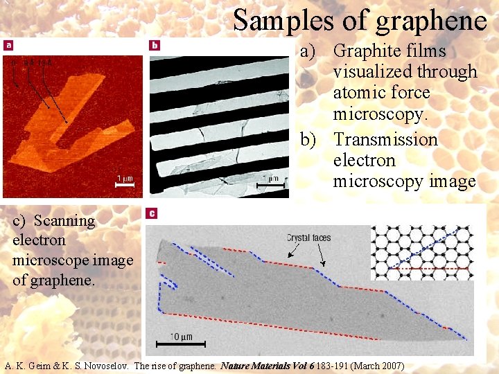
Samples of graphene a) Graphite films visualized through atomic force microscopy. b) Transmission electron microscopy image c) Scanning electron microscope image of graphene. A. K. Geim & K. S. Novoselov. The rise of graphene. Nature Materials Vol 6 183 -191 (March 2007)

Electrons in graphene • Electrons in porbitals above and below plane • p-orbitals become conjugated across the plane • Electrons free to move across plane in delocalized orbitals • Extremely high tensile strength http: //en. wikipedia. org/wiki/Aromaticity -Graphene and graphite are great conductors along the planes.

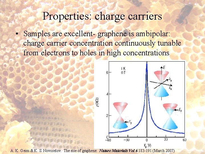
Properties: charge carriers • Samples are excellent- graphene is ambipolar: charge carrier concentration continuously tunable from electrons to holes in high concentrations A. K. Geim & K. S. Novoselov. The rise of graphene. Nature Materials Vol 6 183 -191 (March 2007)

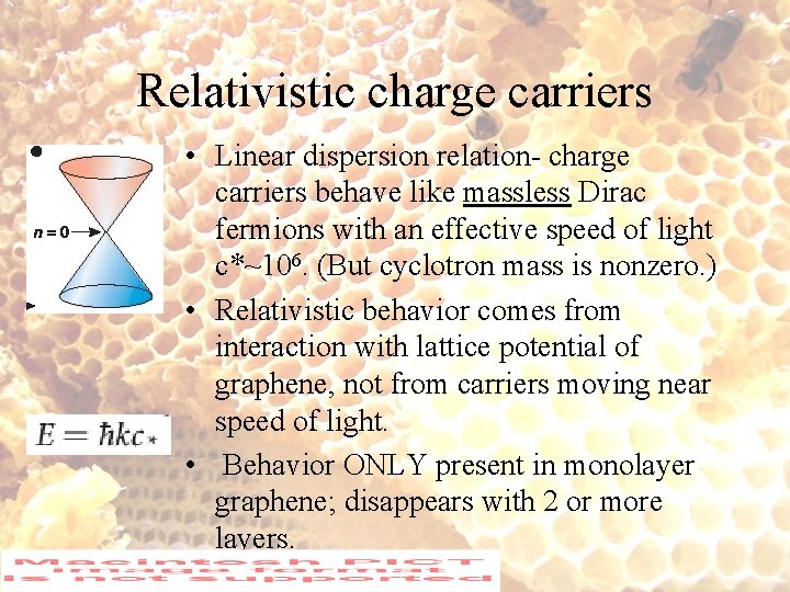
Relativistic charge carriers • Linear dispersion relation- charge carriers behave like massless Dirac fermions with an effective speed of light c*~106. (But cyclotron mass is nonzero. ) • Relativistic behavior comes from interaction with lattice potential of graphene, not from carriers moving near speed of light. • Behavior ONLY present in monolayer graphene; disappears with 2 or more layers.

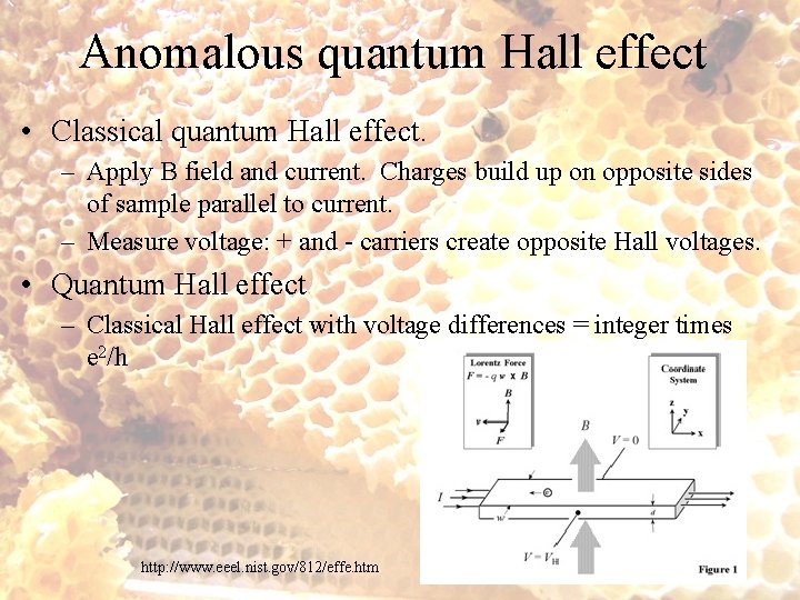
Anomalous quantum Hall effect • Classical quantum Hall effect. – Apply B field and current. Charges build up on opposite sides of sample parallel to current. – Measure voltage: + and - carriers create opposite Hall voltages. • Quantum Hall effect – Classical Hall effect with voltage differences = integer times e 2/h http: //www. eeel. nist. gov/812/effe. htm

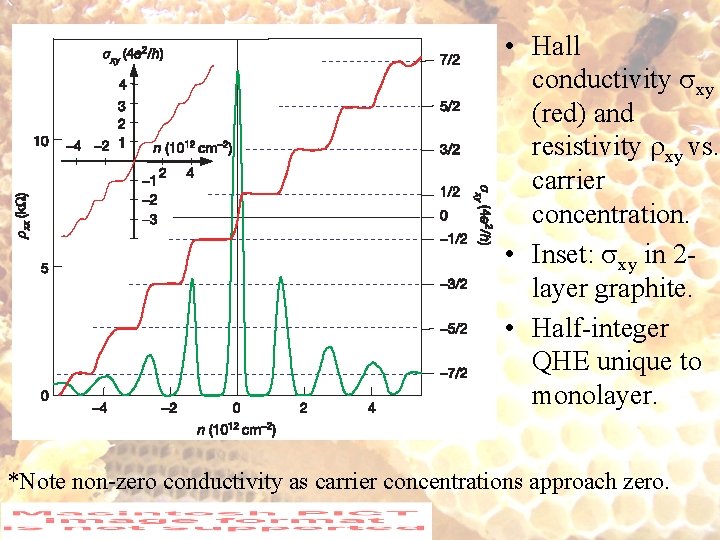
Anomalous quantum Hall effect • Fractional Quantum Hall effect – Quantum Hall effect times rational fractions. Not completely understood. • Graphene shows integer QHE shifted by 1/2 integer • Non-zero conductivity as charge carrier dentsity -> zero.

• Hall conductivity xy (red) and resistivity xy vs. carrier concentration. • Inset: xy in 2 layer graphite. • Half-integer QHE unique to monolayer. *Note non-zero conductivity as carrier concentrations approach zero.

Possible Applications • High carrier mobility even at highest electric-fieldinduced concentrations, largely unaffected by doping= ballistic electron transport over < m distances at 300 K – May lead to ballistic room-temperature transistors. – Ga. Tech group made proof of concept transistor- leaks electrons, but it’s a start. • Energy gap controlled by width of graphene strip. – Must be only 10 s of nm wide for reasonable gap. – Etching still difficult consistently and random edge configuration causes scattering.

Even more applications? • Very high tensile strength • Replacement of nanotubes for cheapness in some applications: composite materials and batteries for improved conductivity • Hydrogen storage • Graphene based quantum computation? Low spin-orbit coupling-> graphene may be ideal as a q-bit.

In Conclusion • Graphene is a novel material with very unusual properties • Easy to make in lab; may prove easy and economical to manufacture (unknown). • Broad range of applications for future research. • Variety of possible practical applications.

Resources • 1. A. K. Geim & K. S. Novoselov. The rise of graphene. Nature Materials Vol 6 183 -191 (March 2007) • 2. N. D. Mermin. Crystalline Order in Two Dimensions. Phys. Rev. 176, 1 250 -253 • 3. H. W. Kroto, J. R. Heath, S. C. O’Brien, R. F. Curl & R. E. Smalley. C 60: Buckminsterfullerene. Nature 318, 162 -163 (1985). • 4. Sumio Iijima. Helical microtubules of graphitic carbon. Nature 354, 56 -58 (1991). • 5. P. R. Wallace. The band theory of graphite. Phys. Rev. 71, 622 -634 (1947). • 6. J. C. Slonczewski & P. R. Weiss. Band structure of graphite. Phys. Rev. 109, 272 -279 (1958). • 7. A. Fasolino, J. H. Los & M. I. Katsnelson. Intrinsic ripples in graphene. Nature Materials 6, 858 -861 (2007) • 8. K. S. Novoselov, et al. Electric field effect in atomically thin carbon films. Science 306, 666 -669 (2004). • 9. K. S. Novoselov, A. K. Geim, S. V. Morozov, D. Jiang, M. I. Katsnelson, I. V. Grigorieva, S. V. Dubonos, & A. A. Firsov. Two-dimensional gas of massless Dirac fermions in graphene. Nature, 438 197 -200 (2005) • 10. Adriaan M. J. Schakel. Relativistic quantum Hall effect. Phys. Rev. D 43, 4 1428 -1431 (1991) • 11. J. Hass, R. Feng, T. Li, X. Li, Z. Zong, W. A. de Heer, P. N. First & E. H. Conrad. Highly ordered graphene for two dimensional electroncs. Applied Physics Letters 89, (2006) • 12. Prachi Patel-Predd. “Ultrastrong paper from graphene”. July 25, 2007. http: //www. technologyreview. com/Nanotech/19097/

End • http: //en. wikipedia. org/wiki/Graphite