Graphene A modern material with unique physical and
- Slides: 23
Graphene A modern material with unique physical and electrical properties that could reshape our future. By: Steven Douglas 4/24/15
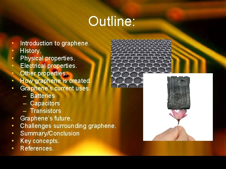
Outline: • • • Introduction to graphene. History. Physical properties. Electrical properties. Other properties. How graphene is created. Graphene’s current uses. – Batteries – Capacitors – Transistors Graphene’s future. Challenges surrounding graphene. Summary/Conclusion Key concepts. References.
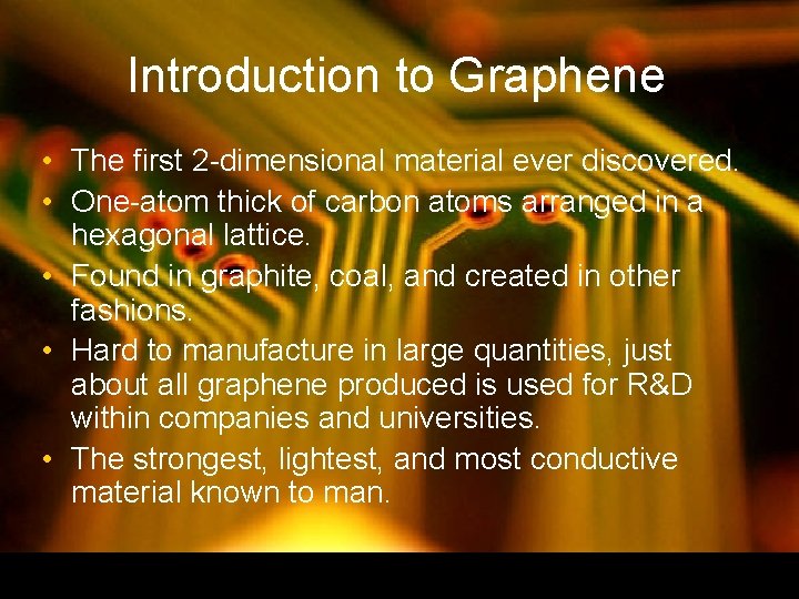
Introduction to Graphene • The first 2 -dimensional material ever discovered. • One-atom thick of carbon atoms arranged in a hexagonal lattice. • Found in graphite, coal, and created in other fashions. • Hard to manufacture in large quantities, just about all graphene produced is used for R&D within companies and universities. • The strongest, lightest, and most conductive material known to man.
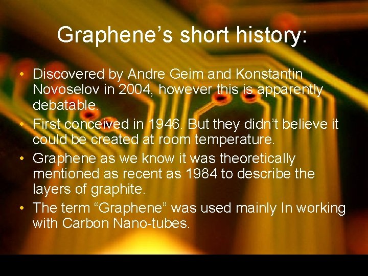
Graphene’s short history: • Discovered by Andre Geim and Konstantin Novoselov in 2004, however this is apparently debatable. • First conceived in 1946. But they didn’t believe it could be created at room temperature. • Graphene as we know it was theoretically mentioned as recent as 1984 to describe the layers of graphite. • The term “Graphene” was used mainly In working with Carbon Nano-tubes.
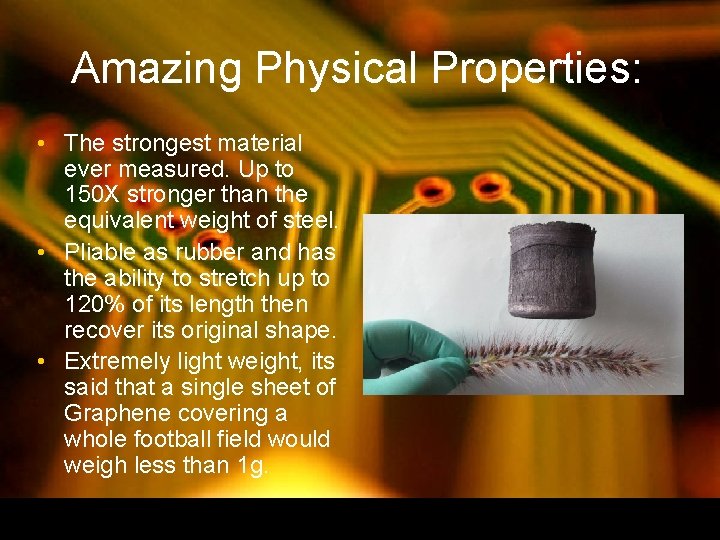
Amazing Physical Properties: • The strongest material ever measured. Up to 150 X stronger than the equivalent weight of steel. • Pliable as rubber and has the ability to stretch up to 120% of its length then recover its original shape. • Extremely light weight, its said that a single sheet of Graphene covering a whole football field would weigh less than 1 g.
Electrical Properties • Graphene is classified as a zero-overlap semimetal, which means that either holes or electrons are charge carriers. • Very high electrical conductivity when exposed to an electric field. • In a vacuum, it had a mobility that was up to 250 X that of Si. Out conducts copper by a thousand times. • Effective mass at the Dirac point is zero for both electrons and holes.
Other Properties: • Only known substance that is completely impermeable to gas. • Graphene oxide reportedly has the ability to attract radioactive material. • Safer creation of “Quantum Dots”. Reduces the price from $1 million a kg to $100 a ton. • Also has some optical properties that are being tested as we speak. • Graphene has the ability to transmit up to 98% of light.
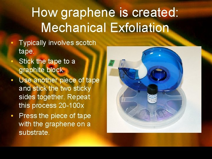
How graphene is created: Mechanical Exfoliation • Typically involves scotch tape. • Stick the tape to a graphite block. • Use another piece of tape and stick the two sticky sides together. Repeat this process 20 -100 x • Press the piece of tape with the graphene on a substrate.
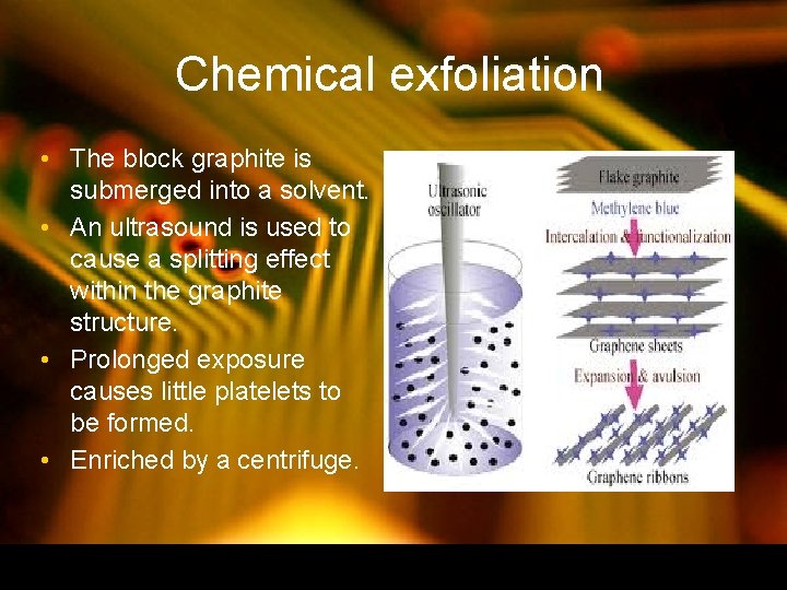
Chemical exfoliation • The block graphite is submerged into a solvent. • An ultrasound is used to cause a splitting effect within the graphite structure. • Prolonged exposure causes little platelets to be formed. • Enriched by a centrifuge.
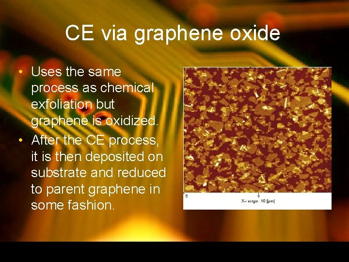
CE via graphene oxide • Uses the same process as chemical exfoliation but graphene is oxidized. • After the CE process, it is then deposited on substrate and reduced to parent graphene in some fashion.
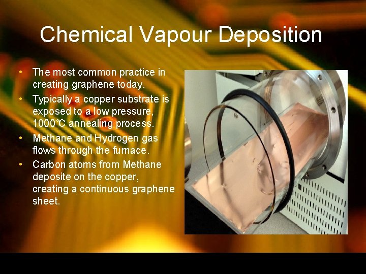
Chemical Vapour Deposition • The most common practice in creating graphene today. • Typically a copper substrate is exposed to a low pressure, 1000˚C annealing process. • Methane and Hydrogen gas flows through the furnace. • Carbon atoms from Methane deposite on the copper, creating a continuous graphene sheet.
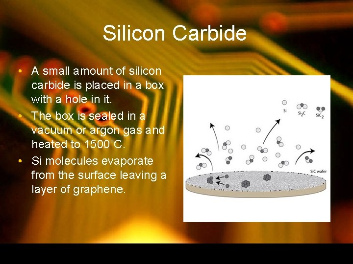
Silicon Carbide • A small amount of silicon carbide is placed in a box with a hole in it. • The box is sealed in a vacuum or argon gas and heated to 1500˚C. • Si molecules evaporate from the surface leaving a layer of graphene.
Graphene’s current uses: • In early 2014 I. B. M announced that it had built the first integrated circuit for wireless devices. • Today a tennis racquet with a graphene layer has been manufactured. • Graphene is an ingredient to conductive inks for printing circuitry. • Samsung is reportedly releasing a screen that employs Graphene to deliver current to the display.
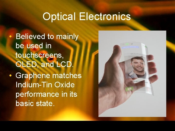
Optical Electronics • Believed to mainly be used in touchscreens, OLED, and LCD. • Graphene matches Indium-Tin Oxide performance in its basic state.
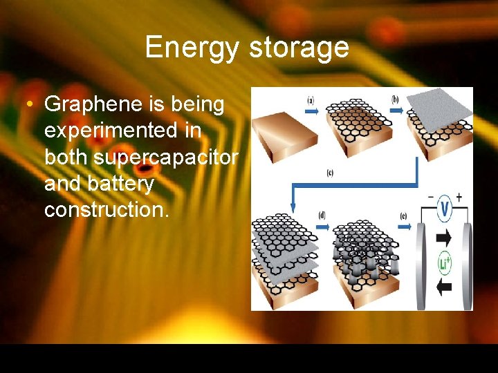
Energy storage • Graphene is being experimented in both supercapacitor and battery construction.
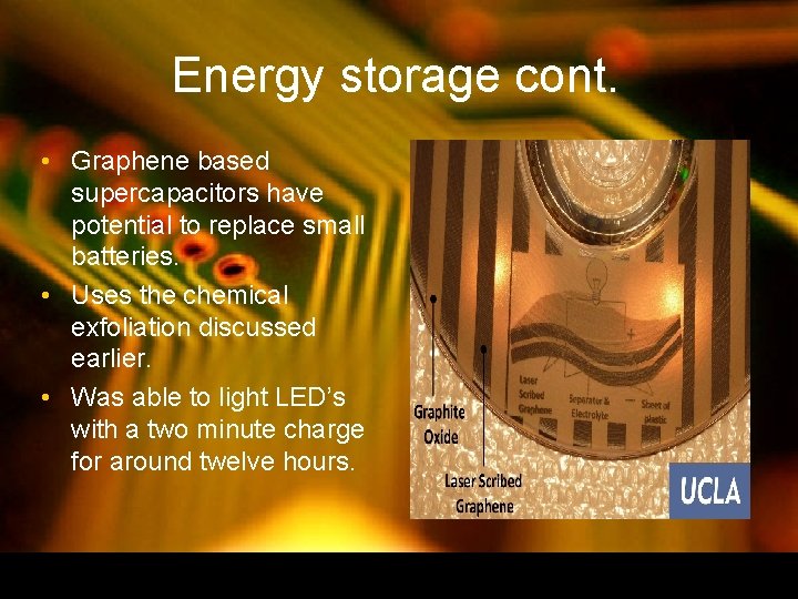
Energy storage cont. • Graphene based supercapacitors have potential to replace small batteries. • Uses the chemical exfoliation discussed earlier. • Was able to light LED’s with a two minute charge for around twelve hours.
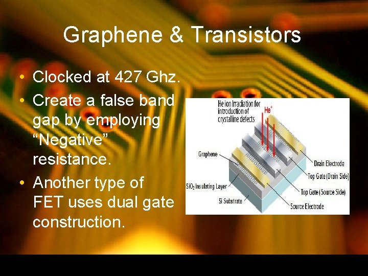
Graphene & Transistors • Clocked at 427 Ghz. • Create a false band gap by employing “Negative” resistance. • Another type of FET uses dual gate construction.
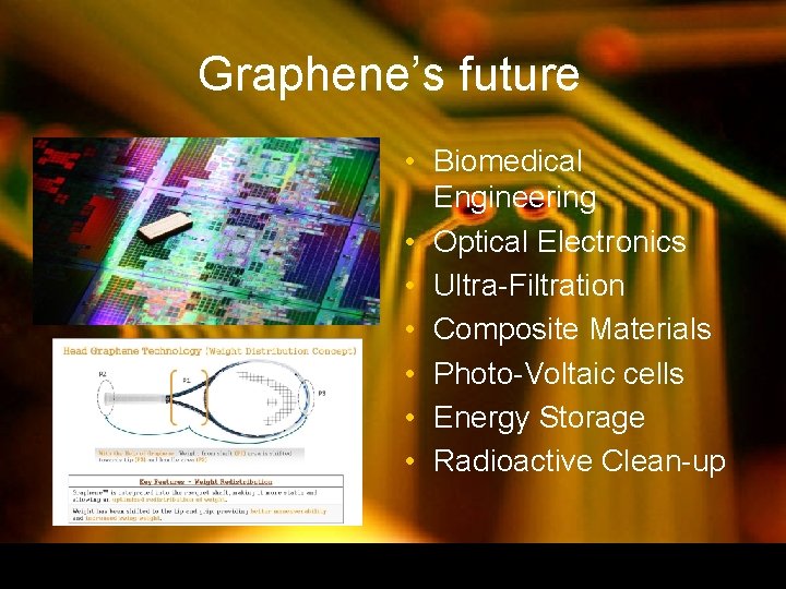
Graphene’s future • Biomedical Engineering • Optical Electronics • Ultra-Filtration • Composite Materials • Photo-Voltaic cells • Energy Storage • Radioactive Clean-up
Challenges Surrounding Graphene • Graphene has no bandwidth, which means it cannot be shut off. • A very hydrophobic material • Very expensive and hard to manufacture for most companies. • When deployed it seemed that the results weren’t duplicated. • Graphene is hard to produce in large usable sheets. Small flakes are what we use to test usually.
Conclusion • Graphene has many obstacles to work around before it can be implemented into today’s technology. • Researchers are suggesting that it’s a matter of months rather than years for the next graphene break through. • Graphene has so many amazing properties, so expect it to impact many types of technologies.
References: • http: //www. sciencedaily. com/releases/2012/09/120910082304. htm • De la Fuente, Jesus. www. graphene. com. 13 April 2015 • Colapinto, John. “Graphene may be the most remarkable substance ever discovered. But what is it for? ”. The New Yorker, 22 December, 2014. Web. 13 April, 2015 • Wang, Brian. ”Graphene Hybrid Supercapacitors storing as much as lead acid batteries which is six times commercial supercapacitors” www. nextbigfuture. com 17 April, 2015. Web 20 April, 2015. • Johnson, Dexter. “Graphene circuit competes head to head with Si technology. ”www. spectrum. ieee. org 3 February, 2014. Web. 20 April, 2014. • Malasarn, Davin. “UCLA Researchers develop new technique to scale up production of graphene micro super capacitors”. www. newsroom. ucla. edu. 19 February, 2013. Web. 20 April, 2015
Key Concepts • The first 2 -D material ever discovered, only measuring 1 -atom thick. • Lightest material ever discovered. • Strongest material ever discovered per unit weight. • Best electrical/thermal conductivity discovered at room temperature. • Currently does not possess a band-gap like a Si gate does.
Questions?