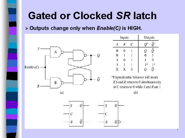
Gated or Clocked SR latch Outputs change only
- Slides: 16
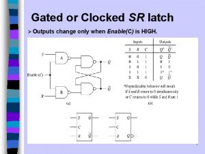
Gated or Clocked SR latch Ø Outputs change only when Enable(C) is HIGH. 1
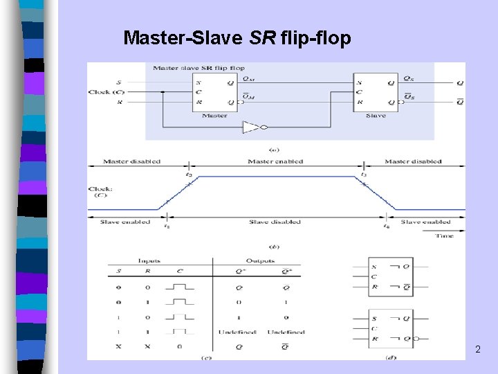
Master-Slave SR flip-flop 2
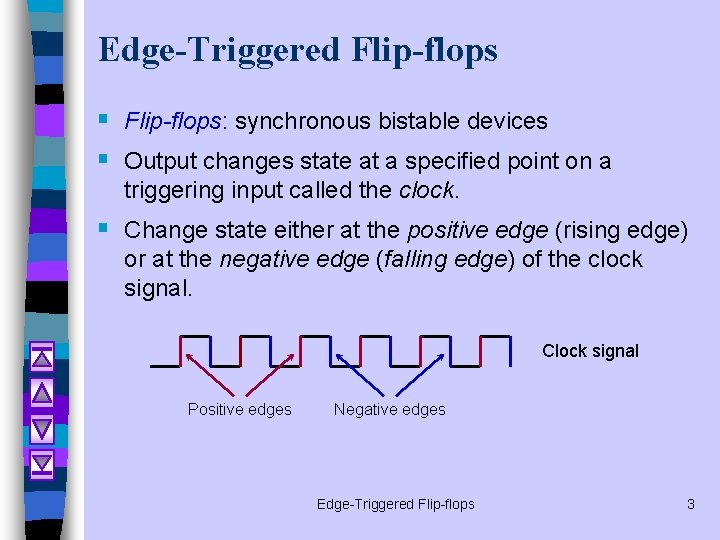
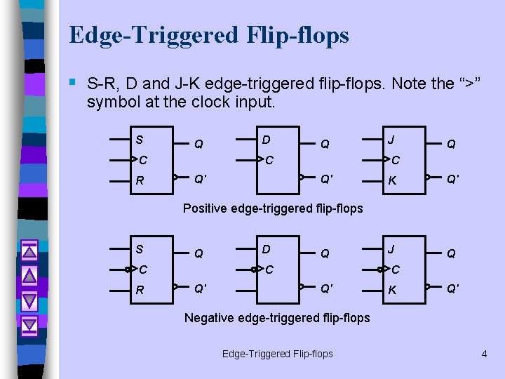
Edge-Triggered Flip-flops § Flip-flops: synchronous bistable devices § Output changes state at a specified point on a triggering input called the clock. § Change state either at the positive edge (rising edge) or at the negative edge (falling edge) of the clock signal. Clock signal Positive edges Negative edges Edge-Triggered Flip-flops 3
Edge-Triggered Flip-flops § S-R, D and J-K edge-triggered flip-flops. Note the “>” symbol at the clock input. S Q C R D Q C Q' J Q C Q' K Q' J Q Positive edge-triggered flip-flops S Q C R D Q C Q' K Q' Negative edge-triggered flip-flops Edge-Triggered Flip-flops 4
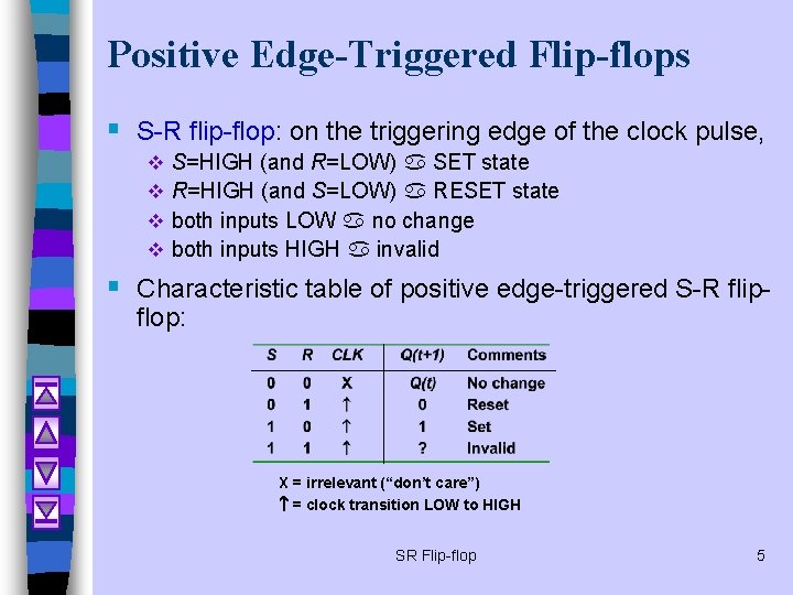
Positive Edge-Triggered Flip-flops § S-R flip-flop: on the triggering edge of the clock pulse, v v S=HIGH (and R=LOW) a SET state R=HIGH (and S=LOW) a RESET state both inputs LOW a no change both inputs HIGH a invalid § Characteristic table of positive edge-triggered S-R flipflop: X = irrelevant (“don’t care”) = clock transition LOW to HIGH SR Flip-flop 5
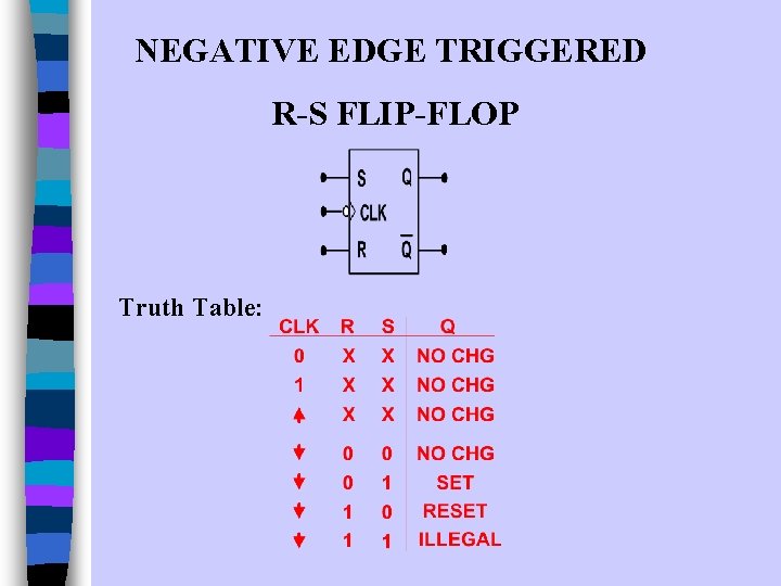
NEGATIVE EDGE TRIGGERED R-S FLIP-FLOP Truth Table:
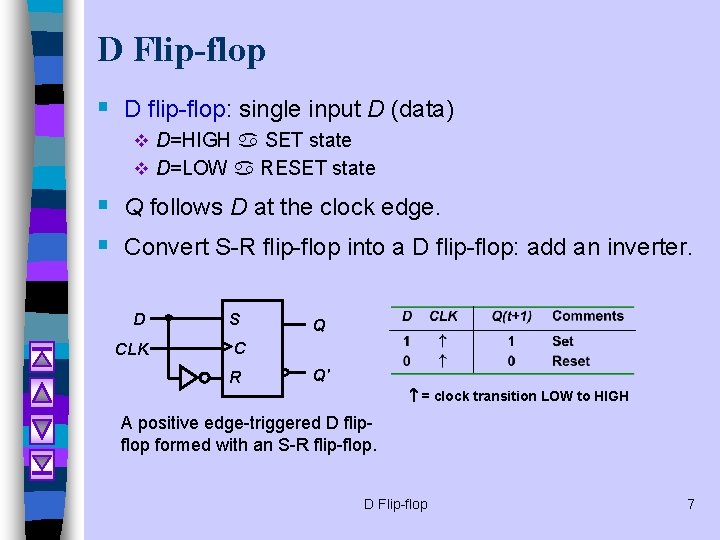
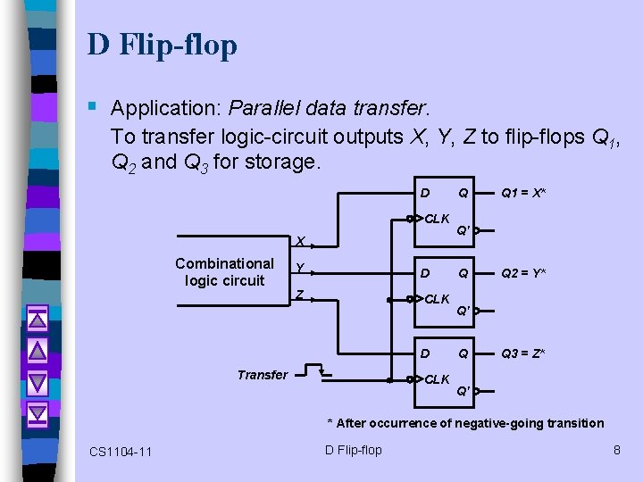
D Flip-flop § D flip-flop: single input D (data) v D=HIGH a SET state v D=LOW a RESET state § Q follows D at the clock edge. § Convert S-R flip-flop into a D flip-flop: add an inverter. D CLK S Q C R Q' = clock transition LOW to HIGH A positive edge-triggered D flipflop formed with an S-R flip-flop. D Flip-flop 7
D Flip-flop § Application: Parallel data transfer. To transfer logic-circuit outputs X, Y, Z to flip-flops Q 1, Q 2 and Q 3 for storage. D CLK X Combinational logic circuit Y D Z CLK D Transfer CLK Q Q 1 = X* Q' Q Q 2 = Y* Q' Q Q 3 = Z* Q' * After occurrence of negative-going transition CS 1104 -11 D Flip-flop 8
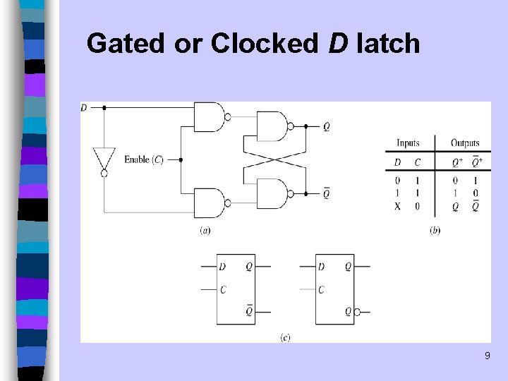
Gated or Clocked D latch 9
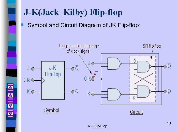
J-K(Jack–Kilby) Flip-flop § This simple JK flip-Flop is the most widely used of all the flip-flop designs and is considered to be a universal flip-flop circuit. § The basic gated SR NAND flip-flop suffers from two basic problems: number one, the S = 0 and R = 0 condition or S = R = 0 must always be avoided, and number two, if S or R change state while the enable input is high the correct latching action may not occur. § Then to overcome these two fundamental design problems with the SR flip-flop, the JK flip-Flop was developed. J-K Flip-Flop 10
J-K(Jack–Kilby) Flip-flop § The sequential operation of the JK flip-flop is exactly the same as for the previous SR flip-flop with the same "Set" and "Reset" inputs. § The difference this time is that the JK flip-flop has no invalid or forbidden input states of the SR Latch (when S and R are both 1). § The JK flip-flop is basically a gated SR flip-flop with the addition of a clock input circuitry that prevents the illegal or invalid output condition that can occur when both inputs S and R are equal to logic level "1". § Due to this additional clocked input, a JK flip-flop has four possible input combinations, "logic 1", "logic 0", "no change" and "toggle". J-K Flip-Flop 11
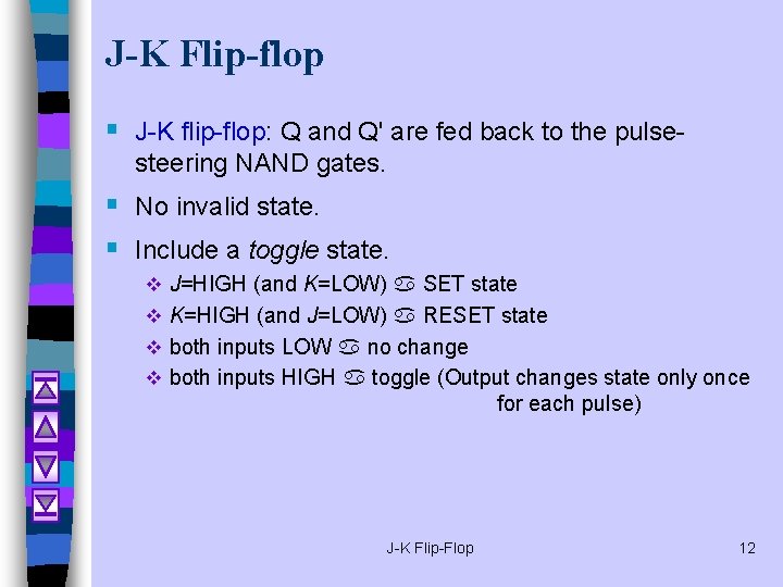
J-K Flip-flop § J-K flip-flop: Q and Q' are fed back to the pulsesteering NAND gates. § No invalid state. § Include a toggle state. v J=HIGH (and K=LOW) a SET state v K=HIGH (and J=LOW) a RESET state v both inputs LOW a no change v both inputs HIGH a toggle (Output changes state only once for each pulse) J-K Flip-Flop 12
J-K(Jack–Kilby) Flip-flop § Symbol and Circuit Diagram of JK Flip-flop: J-K Flip-Flop 13
J-K Flip-flop § Characteristic table. J-K Flip-flop 14
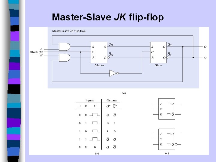
Master-Slave JK flip-flop 1/50 A. Yaicharoen 15
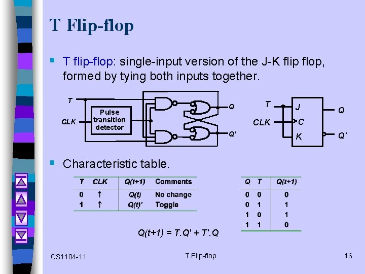
T Flip-flop § T flip-flop: single-input version of the J-K flip flop, formed by tying both inputs together. T CLK Q Pulse transition detector T CLK Q' J Q C K Q' § Characteristic table. Q(t+1) = T. Q' + T'. Q CS 1104 -11 T Flip-flop 16