ESD Protection ESD Stress Models 1 l ESD
- Slides: 16

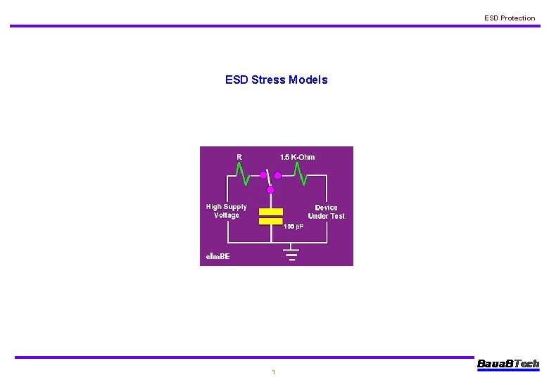
ESD Protection ESD Stress Models 1

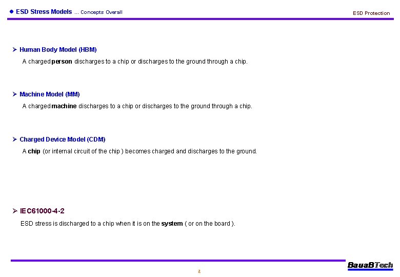
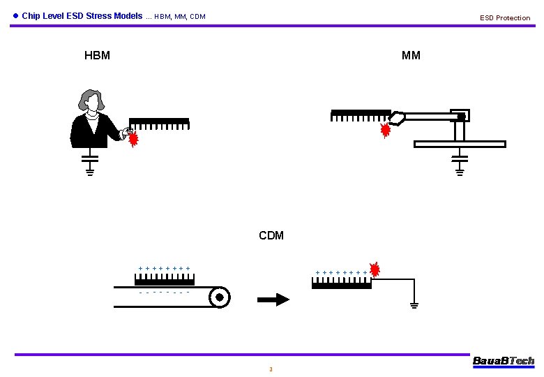
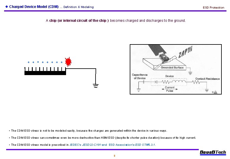
l ESD Stress Models … Concepts Overall ESD Protection Ø Human Body Model (HBM) A charged person discharges to a chip or discharges to the ground through a chip. Ø Machine Model (MM) A charged machine discharges to a chip or discharges to the ground through a chip. Ø Charged Device Model (CDM) A chip (or internal circuit of the chip ) becomes charged and discharges to the ground. Ø IEC 61000 -4 -2 ESD stress is discharged to a chip when it is on the system ( or on the board ). 2

l Chip Level ESD Stress Models … HBM, MM, CDM ESD Protection HBM MM CDM ++++++++ - - - - 3

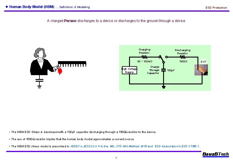
l Human Body Model (HBM) … Definition & Modeling ESD Protection A charged Person discharges to a device or discharges to the ground through a device. Charging Resistor Discharging Resistor 50 ~ 100 MΩ 1500Ω High Voltage Supply Charge Storage Capacitor 100 p. F • The HBM ESD Stress is developed with a 100 p. F capacitor discharging through a 1500 resistor to the device. • The use of 1500 resistor implies that the human body model approximates a current source. • The HBM ESD stress model is prescribed in JEDEC's JESD 22 -A 114, the MIL-STD-883 Method 3015 and ESD Association's ESD STM 5. 1. 4 DUT

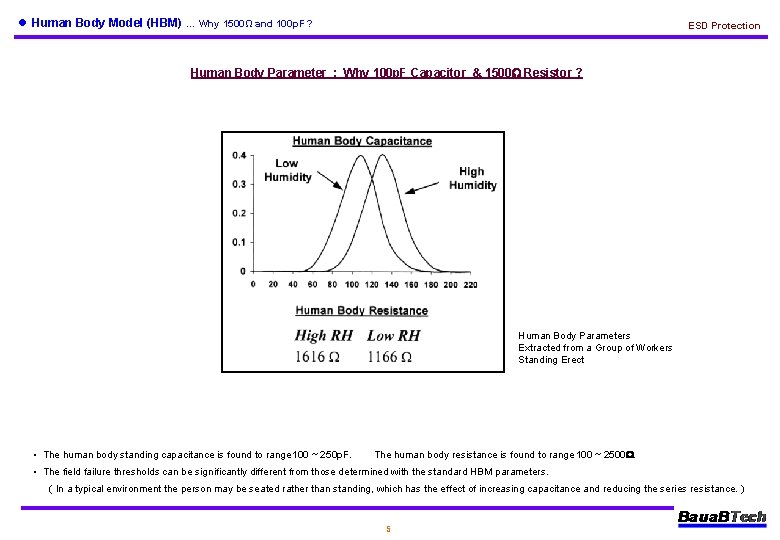
l Human Body Model (HBM) … Why 1500Ω and 100 p. F ? ESD Protection Human Body Parameter : Why 100 p. F Capacitor & 1500 Resistor ? Human Body Parameters Extracted from a Group of Workers Standing Erect • The human body standing capacitance is found to range 100 ~ 250 p. F. The human body resistance is found to range 100 ~ 2500. • The field failure thresholds can be significantly different from those determined with the standard HBM parameters. ( In a typical environment the person may be seated rather than standing, which has the effect of increasing capacitance and reducing the series resistance. ) 5

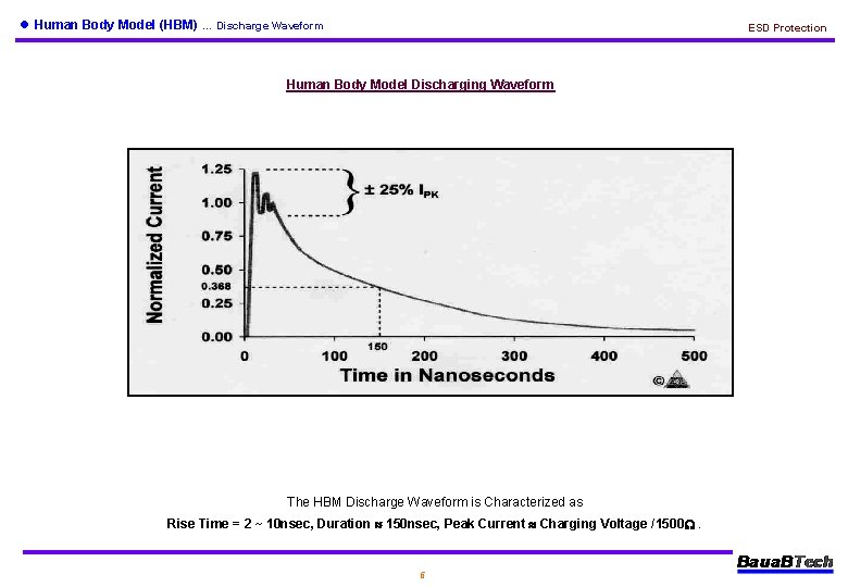
l Human Body Model (HBM) … Discharge Waveform ESD Protection Human Body Model Discharging Waveform The HBM Discharge Waveform is Characterized as Rise Time = 2 ~ 10 nsec, Duration 150 nsec, Peak Current Charging Voltage /1500 . 6

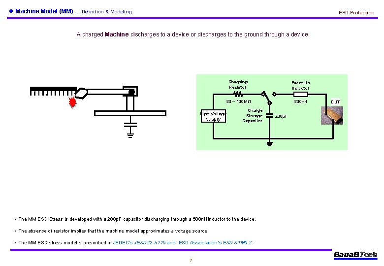
l Machine Model (MM) … Definition & Modeling ESD Protection A charged Machine discharges to a device or discharges to the ground through a device Charging Resistor Parasitic Inductor 50 ~ 100 MΩ 500 n. H High Voltage Supply Charge Storage Capacitor • The MM ESD Stress is developed with a 200 p. F capacitor discharging through a 500 n. H inductor to the device. • The absence of resistor implies that the machine model approximates a voltage source. • The MM ESD stress model is prescribed in JEDEC's JESD 22 -A 115 and ESD Association's ESD STM 5. 2. 7 200 p. F DUT

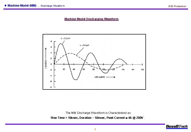
l Machine Model (MM) … Discharge Waveform ESD Protection Machine Model Discharging Waveform The MM Discharge Waveform is Characterized as Rise Time > 10 nsec, Duration ~ 50 nsec, Peak Current 4 A @ 200 V. 8

l Charged Device Model (CDM) … Definition & Modeling ESD Protection A chip (or internal circuit of the chip ) becomes charged and discharges to the ground. + + + + • The CDM ESD stress is not to be modeled easily, because the charges are generated within the device in various ways. • The CDM ESD stress can sometimes even be more destructive than HBM ESD (despite its shorter pulse duration) because of its high current. • The CDM ESD stress model is prescribed in JEDEC's JESD 22 -C 101 and ESD Association's ESD STM 5. 3. 1. 9

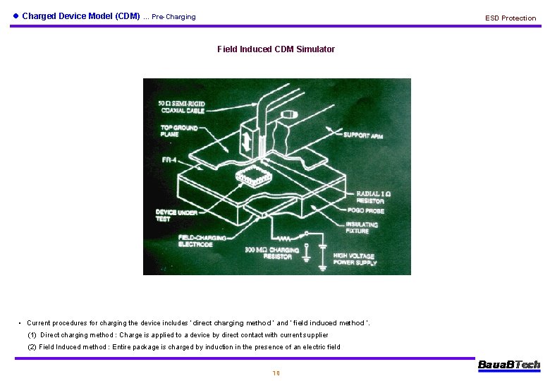
l Charged Device Model (CDM) … Pre-Charging ESD Protection Field Induced CDM Simulator • Current procedures for charging the device includes ‘ direct charging method ’ and ‘ field induced method ’. (1) Direct charging method : Charge is applied to a device by direct contact with current supplier (2) Field Induced method : Entire package is charged by induction in the presence of an electric field 10

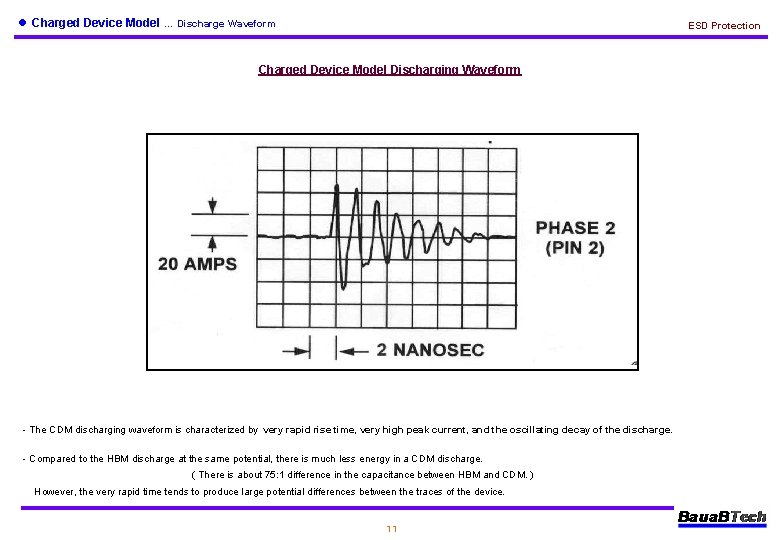
l Charged Device Model … Discharge Waveform ESD Protection Charged Device Model Discharging Waveform - The CDM discharging waveform is characterized by very rapid rise time, very high peak current, and the oscillating decay of the discharge. - Compared to the HBM discharge at the same potential, there is much less energy in a CDM discharge. ( There is about 75: 1 difference in the capacitance between HBM and CDM. ) However, the very rapid time tends to produce large potential differences between the traces of the device. 11

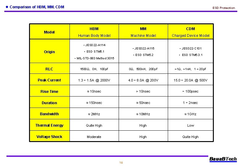
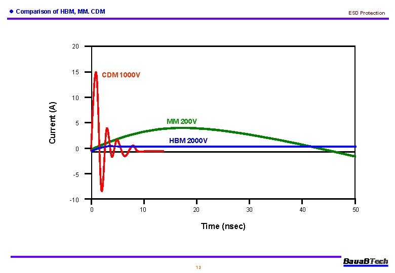
l Comparison of HBM, MM. CDM Model ESD Protection HBM MM CDM Human Body Model Machine Model Charged Device Model • JESD 22 -A 115 • JESD 22 -C 101 • ESD STM 5. 2 • ESD STM 5. 3. 1 • JESD 22 -A 114 Origin • ESD STM 5. 1 • MIL-STD-883 Method 3015 RLC 1500Ω, 0 H, 100 p. F 0Ω, 500 n. H, 200 p. F ~1Ω, ~1 n. H, 1 ~ 20 p. F Peak Current 1. 3 ~ 1. 5 A @ 2000 V 4. 0 ~ 8. 0 A @ 200 V 15. 0 ~ 20. 0 A @ 500 V Rise Time 10 nsec > 10 nsec ~ 100 psec Duration 150 nsec 1 ~ 2 nsec Bandwidth 2 MHz 10 MHz 1 GHz Thermal Energy Quite High Low Voltage Shock Moderate High Quite High 12

l Comparison of HBM, MM. CDM ESD Protection 20 15 CDM 1000 V Current (A) 10 MM 200 V 5 HBM 2000 V 0 -5 -10 0 10 20 30 Time (nsec) 13 40 50

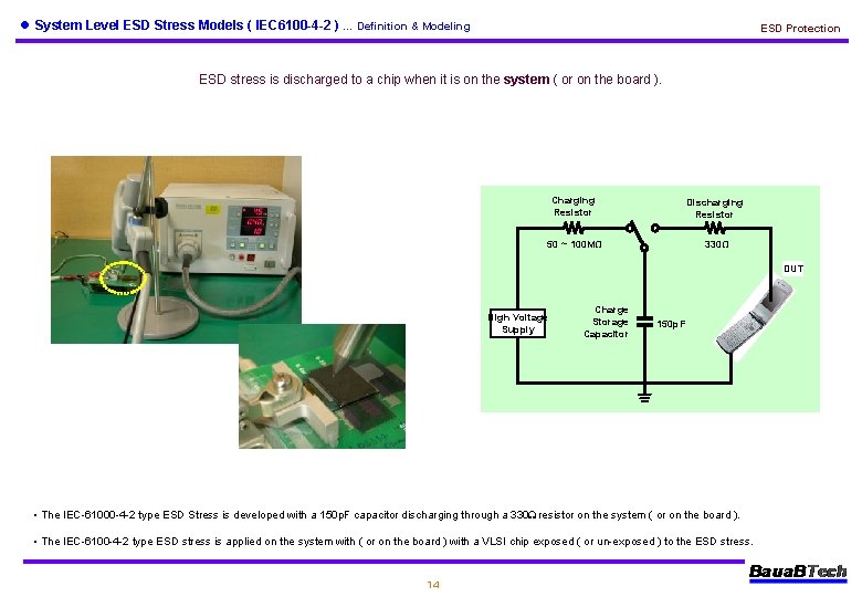
l System Level ESD Stress Models ( IEC 6100 -4 -2 ) … Definition & Modeling ESD Protection ESD stress is discharged to a chip when it is on the system ( or on the board ). Charging Resistor Discharging Resistor 50 ~ 100 MΩ 330Ω DUT High Voltage Supply Charge Storage Capacitor 150 p. F • The IEC-61000 -4 -2 type ESD Stress is developed with a 150 p. F capacitor discharging through a 330 resistor on the system ( or on the board ). • The IEC-6100 -4 -2 type ESD stress is applied on the system with ( or on the board ) with a VLSI chip exposed ( or un-exposed ) to the ESD stress. 14

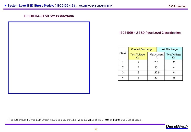
l System Level ESD Stress Models ( IEC 6100 -4 -2 ) … Waveform and Classification ESD Protection IEC 61000 -4 -2 ESD Stress Waveform IEC 61000 -4 -2 ESD Pass Level Classification • The IEC-61000 -4 -2 type ESD Stress’ waveform appears to be the combination of HBM, MM and CDM type ESD stresses. 15

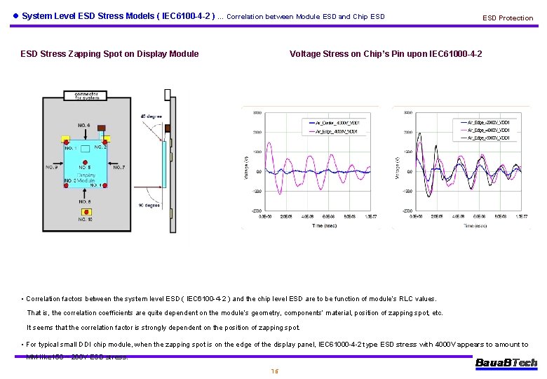
l System Level ESD Stress Models ( IEC 6100 -4 -2 ) … Correlation between Module ESD and Chip ESD Stress Zapping Spot on Display Module ESD Protection Voltage Stress on Chip’s Pin upon IEC 61000 -4 -2 • Correlation factors between the system level ESD ( IEC 6100 -4 -2 ) and the chip level ESD are to be function of module’s RLC values. That is, the correlation coefficients are quite dependent on the module’s geometry, components’ material, position of zapping spot, etc. It seems that the correlation factor is strongly dependent on the position of zapping spot. • For typical small DDI chip module, when the zapping spot is on the edge of the display panel, IEC 61000 -4 -2 type ESD stress with 4000 V appears to amount to MM-like 150 ~ 200 V ESD stress. 16